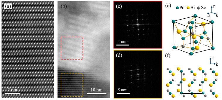
Figure 5.
(a) Atomic-resolution HAADF image of the Bi2Se3 layer far from the Pd/Bi2Se3 interface, showing the clear stacking of Se-Bi-Se-Bi-Se quintuple layers. (b) HAADF image at the Pd/Bi2Se3 interface. A crystalline phase was found to form in the Pd-rich area. (c,d) 2D FFT patterns of the areas indicated by the dashed (c) red and (d) yellow boxes in (b). The lattice constant extracted from the data in (c) is 0.63 nm, fairly close to that of cubic PdBiSe. (e) The unit cell of PdBiSe, with a lattice constant of 0.64 nm. (f) Schematics of the PdBiSe crystal structure. The black box represents the unit cell.

