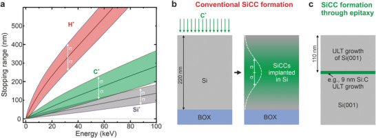
Figure 1.

Intrinsic bottleneck of using ion‐implantation for color center formation. a) Simulated stopping range of Si+, C+ and protons in crystalline Si(001) for different common implantation energies. b) Common fabrication scheme for Si‐color centers (SiCC) consisting of ion‐implantation (here C+) and annealing, leading to a stochastic distribution of emitters in the SOI device layer. c) SiCC formation through molecular beam epitaxy growth at ultra‐low sample temperatures (200–300 °C). Efficient confinement of the emitter position down to the nanoscale through the growth of thin Si:C layers on Si bulk or SOI, overgrown with Si at ULT conditions.
