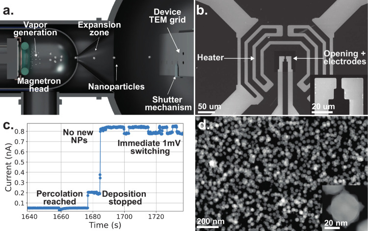
Figure 1.
a. Schematic of NP production via gas-phase synthesis (not to scale). Utilizing a magnetron sputterer and an aggregation chamber, NPs can be produced and deposited onto an electrically monitored (1 mV bias), (S)TEM-compatible chip, as seen in b. In c., the electrical conductivity of the chip is monitored so that one can identify the point of percolation (the first substantial rise in conductivity) and halt the deposition. Note the immediate switching under a 1 mV bias voltage after halting the deposition. A pristine size and deposition rate control yields a percolating network of homogeneously sized NPs seen in d., the HAADF (S)TEM image of a percolating NP film, with a covered area of 67 ± 1%. The inset shows a typical, as-deposited, stellate Mo NP.

