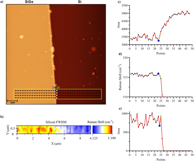
Figure 4.
(a) Tip-enhanced Raman spectroscopy (TERS) map on a 10 × 10 µm2 AFM topography acquired on the edge between the SiGe and Si regions of the SiGe epitaxial-on-SOI device based on 192 points with a distance between each point of 195 nm (the blue and green points represent the positions 24 and 25, respectively); (b) FWHM hyperspectral map obtained by performing a single Lorentzian curve fitting on all the acquisitions; (c) plot of the values of the sum of the areas (peaks at ≈520.5 and ≈ 518 cm–1) obtained by performing a two and three Lorentzian curves fitting to the averaged spectra for the Si and SiGe region, respectively; (d) plot of the spectral position of the strained-Si peak of each averaged spectra; (e) plot of the value of the area of strained-Si peaks of each averaged spectra.

