

Abstract
Phase-pure crystalline chalcostibite (CuSbS2) thin films were prepared by depositing Cu/Sb/Cu metal stacks using a thermal evaporation method, followed by sulfurization at 400 oC and 430 oC for different durations. The investigation revealed the formation of a dominant orthorhombic CuSbS2 phase accompanied by a minor Sb2S3 phase in the film stacks sulfurized at 400 oC for 10–60 min. Extending the reaction time to 90 min triggered a decrease in the Sb2S3 phase and the emergence of an additional famatinite (Cu3SbS4) phase alongside the dominant CuSbS2 phase. Sulfurization of the film stack at 430 oC for 10 min similarly produced a Cu3SbS4 secondary phase. When sulfurization was maintained beyond 30 min at 430 oC, it resulted in phase-pure CuSbS2 films, characterized by a crystalline grain size of 25.9 nm, direct bandgap of 1.41 eV, and hole mobility ranging from 0.6–1.0 cm2V−1s−1. Thin film solar cells fabricated using the CuSbS2 absorbers grown at 430 oC for 30–90 min displayed exceptional device efficiency due to the formation of phase-pure and highly crystalline films. Specifically, solar cells fabricated using the CuSbS2 absorber sulfurized for 60 min demonstrated a peak device efficiency of 2.2%, featuring an open-circuit voltage of 546.6 mV, short-circuit current density of 12.8 mA/cm2, and a fill factor of 31.3%. This study provides a reference for preparing highly crystalline CuSbS2 thin films for efficient solar cells.
Keywords: CuSbS2 solar cells, Two-stage process, Thermal evaporation, DRS, Raman
1. Introduction
In recent decades, the growing demand for energy resources and diminishing appeal of fossil fuels have spurred extensive research into alternative energy sources, particularly renewable and pollution-free sources. Solar energy, in particular has emerged as a highly attractive option among the renewable and eco-friendly alternatives. Consequently, various solar thermal, and photovoltaic (PV) energy systems have been developed to harness the immense potential of sunlight. While single and multi-crystalline silicon (Si)-solar modules with efficiencies of 24.4% [1], [2] are commercially available, there is an urgent need for reduced costs and enhanced efficiency in Si PV technology [2]. Thin-film solar cells, a promising alternative, utilize a thin 1 μm absorber layer in contrast to the 100–200 μm thick Si-wafer used in traditional Si-solar cells. Thin-film solar cells, including those based on CdTe, Cu(In,Ga)Se2 (CIGS) have been developed, achieving efficiencies exceeding 20%. Additionally, amorphous-Si (a-Si) solar cells have realized efficiencies up to 12% [3]. Notably, CIGS solar cells have set efficiency records, reaching 23.35% for small areas and 19.2% for modules [3]. Despite these advancements, the use of rare and costly elements in CIGS hinders its cost-effectiveness for mass production. As a result, researchers have turned their attention to alternative semiconductors. Among these, the kesterite family stands out for its use of abundant, non-toxic precursor materials. Recent advancements in kesterite-based solar cells achieved a peak conversion efficiency of 14.9%, as verified by the National Renewable Energy Laboratory (NREL) [4]. Another material, Cu2SnS3 (CTS), that is akin to Cu2ZnSnS4 (CZTS) has also garnered significant interest. Research involving a germanium (Ge) doped CTS absorber reported a conversion efficiency of 6.7% [5]. Similarly, tin sulfide (SnS)-based thin-film solar cells are promising. For example, an SnS-based device exhibits an efficiency of 4.3% using an atomic-layer deposition-grown absorber [6]. Copper(Cu)–antimony(Sb)–sulfur(S) ternary compounds have recently been recognized as potential materials for solar cells due to their unique optical and electrical properties. These compounds are particularly attractive because of their composition of non-toxic and earth-abundant elements. Cu-Sb-Sulfides showcase direct optical bandgaps ranging from 0.42 to 1.85 eV, coupled with a substantial optical absorption coefficient (α ≥105 cm−1) and inherent p-type electrical conductivity. Furthermore, when compared to CIGS, CZTS, and CTS systems, the Cu-Sb-S compounds can be processed at lower temperatures. This offers a distinct advantage in producing high-quality Cu-Sb-S films more efficiently at reduced temperatures.
The Cu-Sb-S system is characterized by four stable phases: chalcostibite (CuSbS2), skinnerite (Cu3SbS3), famatinite (Cu3SbS4), and tetrahedrite (Cu12Sb4S13). Notably, CuSbS2 has been the focal point of much research due to its direct optical bandgap of 1.5 eV, high optical absorption coefficient, and inherent p-type electrical conductivity. There have been significant efforts to fabricate CuSbS2 thin films employing various deposition techniques. These methods include sputtering [7], evaporation [8], [9], electrodeposition [10], spin coating [11], [12], spray pyrolysis [13], chemical bath deposition (CBD) [14], and two-stage processes [15], [16], [17], each under varied conditions. Despite these efforts, CuSbS2-based solar cells have been limited by modest device performance, reaching a conversion efficiency of approximately 3% [17], [18]. Several factors potentially contribute to this limited efficiency include the emergence of secondary phases, specific crystallographic orientation, morphology, the thickness of the absorber layer, and decreased hole mobility in the CuSbS2 films [19]. Consequently, gaining a comprehensive understanding of the growth dynamics, formation mechanism, compositional control, morphology, and the optical and electrical attributes of the CuSbS2 absorber layer is pivotal to enhancing the material quality and ultimately achieving optimal device efficiency.
The two-stage deposition process is notable for its scalability and high throughput, having yielded the highest conversion efficiencies for CZTS and CTS films [5], [20]. This method involves the initial formation of a precursor layer, followed by either annealing or sulfurization. Both the deposition of the precursor layer and the sulfurization step are crucial for achieving high-quality films. In a previous study, we employed this approach for CuSbS2 thin films [21], preparing Sb2S3 and Cu stacks via CBD and sputtering, and then annealing them in an S atmosphere. Nonetheless, using different techniques for precursor layer deposition can be time consuming and less efficient. Hence, in this study, we transitioned to thermal evaporation for depositing the Sb and Cu metallic layers, which offers speed and precise thickness. However, only a few studies have addressed CuSbS2 thin film growth through the chalcogenization of Cu-Sb precursors using this method, primarily due to challenges related to Sb evaporation. For instance, Colombara et al. [22] achieved complete conversion of the Cu-Sb precursors to CuSbS2 at 350 oC but observed binary phase formation at lower temperatures. Similarly, Wan et al. [23] utilized a dual-temperature, two-stage co-evaporation technique in their preparations. In our study, we also adopted a two-stage method to produce large-grained, phase-pure CuSbS2 films. To address the re-evaporation issues linked to the low melting point of Sb, and ensure strong film adhesion, we sandwiched the Sb layer between two Cu layers of different thicknesses, following a Cu/Sb/Cu sequence. We also optimized the sulfurization temperature and duration to achieve CuSbS2 films with ideal grain growth for solar cell. Finally, we fabricated thin-film solar cells from the optimally prepared CuSbS2 absorber and assessed their operational efficacy.
2. Experimental methods
The thermal evaporation of Cu and Sb was commenced with the cleaning of the chromic acid-soaked soda-lime glass substrates with a soap solution. This was followed by ultrasonication in acetone, ethanol, and deionized (DI) water for 5 min. A two-source thermal evaporation unit was used for the evaporation of the precursor layer. A 4N pure Cu and Sb slug placed in a tungsten boat was used as the source material. A quartz crystal thickness monitor was used to measure the thickness of the precursor layers at the time of deposition. From the mass density calculations, the thicknesses of Cu and Sb required to form 1-μm thick films were estimated to be 130 and 360 nm, respectively, as illustrated in the following equation: Cu (130 nm) + Sb (360 nm) + 2 S → CuSbS2 (1000 nm). The precursor thicknesses of Cu and Sb were slightly increased to 155 and 400 nm, respectively, to obtain CuSbS2 thickness exceeding 1 μm. First, 75 nm of the Cu precursor layer was evaporated; this was followed by the sequential evaporation of 400 nm Sb and 80 nm Cu layers onto glass substrates maintained at room temperature. The Cu was evaporated at a rate of 3 Å/s, while Sb was evaporated at a rate not exceeding 4 Å/s due to its low melting point. Notably, higher evaporation rates for Sb would result in lumps and pinholes after sulfurization. The evaporated Cu/Sb/Cu stacks were sulfurized by placing them in a graphite box and loading them into a quartz tubular furnace. Elemental S powder loaded in a graphite box was used as the S source. The quartz tube was filled with nitrogen gas (N2) at atmospheric pressure to ensure a higher S pressure within the box, thus reducing the loss of elements from the stack during sulfurization. The furnace was heated at 10 oC/min to reach the desired sulfurization temperatures (400 and 430 oC), and sulfurization was conducted for 10, 30, 60, and 90 min. Following the sulfurization process, the samples were cooled to 250 oC at 2 oC/min and then allowed to naturally cool to room temperature.
Subsequently, thin-film solar cells were fabricated with an SLG/Mo/CuSbS2/CdS/ZnO/ITO/Ag configuration using CuSbS2 absorbers grown at the optimized sulfurization temperature of 430 oC for 30, 60, and 90 min durations. A chemical bath deposition method (CBD) was used to deposit a 70 nm thick CdS buffer layer onto the CuSbS2 layer [24]. Following the CdS deposition, the CuSbS2/CdS layers were subjected to annealing at 300 oC under N2 to improve the junction [25]. Intrinsic ZnO (40 nm) and ITO (300 nm) window layers were deposited using radio-frequency magnetron sputtering. The top Ag grid contacts were thermally evaporated with a thickness of 200 nm. Finally, the solar cells (0.36 cm2) were separated via mechanical scribing for testing.
The crystal structure and phase-purity of the CuSbS2 films sulfurized at 400 and 430 oC for different durations were evaluated by acquiring grazing incidence X-ray diffraction (GIXRD) patterns using a PANalytical X-ray diffractometer with a Cu Kα (0.15406 nm) source at an incident angle (ω) of 3o. A Thermo Fisher Scientific confocal micro-Raman spectrometer (Nicolet 6700) was used to perform the phase analysis of the films. An X-ray photoelectron spectrometer (XPS; Thermo Fisher Scientific, K-Alpha spectrometer) was used to evaluate the oxidation states of the elements in the films. The XPS spectra were obtained in the range of 0−1200 eV using an Al Kα source calibrated to the C1s line. Field emission scanning electron microscope (FESEM; Hitachi S-4800) was used to record the surface morphologies and cross-sections of the films. An energy dispersive X-ray spectroscopy (EDAX) was performed to determine the elemental composition of the films. A Cary 5000 UV-Vis-NIR double-beam spectrophotometer was used to record the spectral transmittance of the films in the range of 300–2500 nm. An ECOPIA Hall measurement system (HMS-3000, VER 3.53) was used to determine the electrical properties of the films. The performance of the prepared CuSbS2 solar cells was evaluated by recording current density versus voltage curves using a portable solar simulator (Model: PEC-L01) under AM 1.5 G condition [24].
3. Results and discussion
3.1. Elemental analysis
The EDAX elemental compositions and thicknesses of the CuSbS2 films developed by sulfurizing the Cu/Sb/Cu stacks at 400 and 430 oC for different durations are listed in Table 1. The stoichiometric atomic percentages of Cu, Sb, and S in CuSbS2 are 25, 25, and 50%, respectively. As shown in Table 1, the elemental composition of the stack sulfurized at 400 oC for 10 min was slightly Cu-poor and Sb-rich, which was within the accuracy limits of the EDS analysis (± 5 at%). Upon increasing the sulfurization time from 30 to 90 min, the composition of Cu was slightly enhanced and that of Sb decreased due to gradual loss of Sb with increasing duration. The Cu/Sb ratio significantly increased from 0.79 to 0.95, and the S/(Cu+Sb) ratio remained close to 1.0, as the sulfurization duration increased from 10 to 90 min. The CuSbS2 films prepared by sulfurizing the stacks at 430 oC for all durations exhibited near-stoichiometric composition. The Cu/Sb and S/(Cu+Sb) ratios were close to one under all conditions. This indicates that a sulfurization temperature of 430 oC was ideal for obtaining near-stoichiometric compositions of the CuSbS2 thin films. As listed in Table 1, the thickness of CuSbS2 increases from 1.32 to 1.35 μm as the sulfurization duration increases from 10 to 60 min at 400 oC. Conversely, it decreases to 1.2 μm at 90 min of sulfurization. Similarly, the thickness of the films increases from 1.16 to 1.21 μm as sulfurization duration increases from 10 to 60 min at 430 o, whereas it decreases to 1.19 μm at 90 min of sulfurization. The decrease in film thickness after 90 min of sulfurization at both temperatures could be attributed to the loss of material during longer sulfurization periods.
Table 1.
Elemental composition and thicknesses of the CuSbS2 films developed by sulfurizing Cu/Sb/Cu stacks at 400 and 430 oC for different durations.
| Sulfurization temperature | Sulfurization duration (min) | At. percent |
Ratio |
Thickness (μm) | |||
|---|---|---|---|---|---|---|---|
| Cu | Sb | S | Cu/Sb | S/(Cu+Sb) | |||
| 10 | 22.1 | 27.9 | 50.0 | 0.79 | 1.00 | 1.32 | |
| 400 oC | 30 | 22.2 | 27.0 | 50.8 | 0.82 | 1.03 | 1.31 |
| 60 | 22.9 | 26.0 | 51.0 | 0.88 | 1.04 | 1.35 | |
| 90 | 24.4 | 25.6 | 50.0 | 0.95 | 1.00 | 1.20 | |
| 10 | 25.8 | 25.0 | 49.2 | 1.03 | 0.97 | 1.16 | |
| 430 oC | 30 | 25.2 | 25.2 | 49.6 | 1.00 | 0.98 | 1.19 |
| 60 | 24.7 | 25.8 | 49.5 | 0.96 | 0.98 | 1.21 | |
| 90 | 25.2 | 24.2 | 50.6 | 1.04 | 1.02 | 1.19 | |
3.2. XRD analysis
The crystal structures and phases of the films were evaluated by XRD. Fig. 1 displays the grazing incidence-XRD (GIXRD) patterns of the CuSbS2 films prepared by sulfurizing the Cu/Sb/Cu stacks at 400 and 430 oC for different durations. A standard stick pattern of CuSbS2 is inserted at the bottom of Figs. 1(a) and (b) to distinguish its peaks. The stack sulfurized at 400 oC for 10 min showed diffraction peaks corresponding to the CuSbS2 phase (JCPDS Card No. 01-088-0822) with a dominant peak at (031). Three low-intensity peaks corresponding to the Sb2S3 secondary phase appear at 15.65o, 17.56o, and 33.47o (marked with * symbols), along with those of CuSbS2. The crystal structure of CuSbS2 was determined to be orthorhombic, with lattice parameters a = 0.616 nm, b = 0.382 nm, and c = 1.1448 nm, matching the reported lattice parameters of CuSbS2 (JCPDS Card No. 01-088-0822). The full width at half maximum (FWHM) of the (111) peak was 0.394o. Upon increasing the sulfurization time from 30 to 60 min, Sb2S3 remained in the secondary phase, and the broadening of the (111) peak decreased from 0.3936 to 0.344o, indicating an increase in the crystallite size of the films. The presence of the Sb2S3 secondary phase in the films sulfurized at 400 oC for 10, 30, and 60 min might explain the slight Sb-rich composition observed in the elemental analysis. Further increasing the sulfurization time to 90 min eliminated the Sb2S3 secondary phase due to the loss of Sb during longer sulfurization duration, and peaks related to the Cu3SbS4 phase emerged at 2θ positions of 18.43 and 33.31o (marked with # symbol). The (111) peak became dominant when the film stack was sulfurized for 90 min.
Figure 1.

GIXRD patterns of the CuSbS2 films developed by sulfurizing Cu/Sb/Cu stacks at (a) 400 and (b) 430 oC for different durations.
The stack sulfurized at 430 oC for 10 min (Fig. 1(b)) exhibited peaks corresponding to the dominant CuSbS2 phase and minor Cu3SbS4 secondary phase. Upon increasing the sulfurization time from 30 to 90 min, the peaks corresponding to the Cu3SbS4 phase were completely diminished and the films became phase-pure CuSbS2. The FWHM of the (111) peak was found to be 0.394o for the films sulfurized for 10 min and decreased to 0.344o after 30 min of sulfurization owing to the increased crystallite size.
The crystallite size (D) was estimated after correcting for instrumental peak broadening, using Scherrer's formula [26]. The lattice strain (ϵ) and dislocation density (δ) are determined using the following equations and values are listed in Table 2:
Table 2.
Structural parameters of the CuSbS2 thin films developed by sulfurizing Cu/Sb/Cu stacks at 400 and 430 oC for different durations.
| Sulfurization temperature | Duration (min) | 2θ (degrees) | (degrees) | Crystallite size D (nm) | Strain ϵx10−3 | Dislocation density δx10−3 (nm−2) |
|---|---|---|---|---|---|---|
| 400 oC | 10 | 28.39 | 0.382 | 22.4 | 0.48 | 1.99 |
| 30 | 28.39 | 0.382 | 22.4 | 0.48 | 1.99 | |
| 60 | 28.40 | 0.331 | 25.9 | 0.19 | 1.49 | |
| 90 | 28.41 | 0.331 | 25.9 | 0.19 | 1.49 | |
| 430 oC | 10 | 28.39 | 0.382 | 22.4 | 0.48 | 1.99 |
| 30 | 28.41 | 0.331 | 25.9 | 0.19 | 1.49 | |
| 60 | 28.41 | 0.331 | 25.9 | 0.19 | 1.49 | |
| 90 | 28.43 | 0.331 | 25.9 | 0.19 | 1.49 | |
D = ——— (1)
ϵ = ——— (2)
δ = ——— (3)
Here, k denotes the shape factor, λ represents the X-ray wavelength, θ is the Bragg angle, and denotes the relative peak broadening ( = , where denotes the FWHM of the measured intense diffraction peak, and denotes the FWHM (0.096o) of the intense diffraction peak of Si standard sample).
The crystallite size of the films sulfurized for 10 and 30 min durations at 400 oC was 22.4 nm, which increased to 25.9 nm as the sulfurization duration was increased from 60 to 90 min. The crystallite size of the film sulfurized at 430 oC for 10 min was 22.4 nm, which increased to 25.9 nm after 30 min of sulfurization duration. The lattice strain was found to decrease from 0.48 × 10⁻³ to 0.19 × 10⁻³ upon increasing the sulfurization duration from 10 to 90 min at 400 and 430 oC, respectively. This indicates that the increased sulfurization duration reduces the strain in the CuSbS2 films at 400 and 430 oC. The dislocation density of the films was also found to decrease from 1.99 × 10⁻³ to 1.49 × 10⁻³ nm−2 upon increasing the sulfurization duration from 10 to 90 min at 400 and 430 oC, respectively, owing to the increased crystallite size.
3.3. Raman spectroscopy analysis
Raman spectroscopy was used as a complementary technique for phase analysis. Fig. 2 illustrates the Raman spectra of the CuSbS2 films developed by sulfurizing the stacks at 400 oC and 430 oC for 10, and 60 min. The Raman spectra of the films sulfurized at 400 oC for 10 and 60 min (Fig. 2(a)) showed an intense peak at 338 cm−1 along with minor humps at 105, 145, 166, and 256 cm−1. The reported Raman modes for CuSbS2 appeared at 100, 150, 165, 254, and 337–332 cm−1 [16], [27]. The Raman modes exhibited by our samples match the reported Raman modes of CuSbS2. However, the Sb2S3 secondary phase that appearing in the XRD spectra of these films was not reflected in the Raman spectra, which could be due to the detection limit of the Raman probe depth (approximately 100 nm). This suggests that the Sb2S3 phase formed an interior toward the bottom of the film; hence, its presence was not detected in the Raman spectra. The Raman spectra of the films developed by sulfurizing the stacks at 430 oC for 10 and 60 min also exhibit peaks corresponding to CuSbS2. The modes corresponding to Cu3SbS4, which appeared as a secondary phase in the XRD pattern of the film sulfurized for 10 min, were not observed because of the limited depth of the Raman probe. The variation in the intensities of the Raman modes for different sulfurization durations can be attributed to the variation in the crystallinity of the films.
Figure 2.

Raman spectra of the CuSbS2 films developed by sulfurizing Cu/Sb/Cu precursors at (a) 400 oC and (b) 430 oC for 10 and 60 min.
3.4. XPS analysis
To determine the valence states of the elements present in the films, we performed XPS measurements on CuSbS2 films developed by sulfurizing the stacks at 430 oC for 60 min. Survey and narrow scan XPS spectra of Cu, Sb, and S are shown in Fig. 3. The survey scan (Fig. 3(a)) exhibited signals corresponding to Cu, Sb, S, carbon (C), and Ar. The C and Ar signals could be due to surface contamination of the film. The narrow scan of the Cu2p shown in Fig. 3(b) exhibited two peaks at 932.3 eV and 952.1 eV corresponding to Cu2p3/2 and Cu2p1/2, respectively. The peak positions and their separation of 19.8 eV indicate that the oxidation state of Cu was +1 [23], [28]. The narrow scan of Sb3d (Fig. 4(c)) exhibited two peaks at 529.3 and 538.6 eV with a separation of 9.3 eV corresponding to Sb3d5/2 and Sb3d3/2, respectively. The peak positions and their separation represent the oxidation state of Sb as +3 [23], [28]. The narrow scan in Fig. 3(d) showed two peaks at positions 161.7 and 162.8 eV with a separation of 1.1 eV related to S2p3/2 and S2p1/2, respectively, indicating that the oxidation state of S was -2 [23], [28]. Therefore, the oxidation state of the elements present in the films was Cu+1Sb+3S.
Figure 3.

(a) Survey scan and narrow scan XPS spectra of (b) Cu, (c) Sb, and (d) S of CuSbS2 films developed by sulfurizing Cu/Sb/Cu stacks at 430 oC for sulfurization time of 60 min.
Figure 4.

Cross sectional FESEM image of Cu/Sb/Cu stack before sulfurization, and the surface morphology and cross sectional images of CuSbS2 films developed by sulfurizing the stacks at 400 and 430 oC for different durations.
3.5. Microstructural analysis
The cross sectional FESEM image of the Cu/Sb/Cu stack before sulfurization and the microstructures of the films developed by sulfurizing the stacks at 400 oC and 430 oC for different durations are shown in the FESEM images in Fig. 4. The cross section of the metal stack showed the formation of densely packed Cu, Sb, and Cu layers uniformly coated with thicknesses of 75, 400, and 80 nm, respectively. The surface morphology of the Cu/Sb/Cu stack sulfurized at 400 oC for 10 min exhibited uniform, dense, and distinct round particles with an average size of approximately 500 nm. The cross sectional image shown in the inset reveals the formation of a compact and well adherent film with particles extending vertically to a thickness of 1.32 μm. Increasing the sulfurization time from 30 to 60 min enhanced the uniformity and compactness, and the average particle size increased from 1.0 to 1.5 μm. The particle size also increased with the thickness, as shown in the inset. A further increase in the sulfurization time to 90 min reduced the average particle size to 1.0 μm, probably due to the re-evaporation of the elements from the film as a result of the longer sulfurization time. The cross sectional images also revealed a decrease in the particle size along the thickness with increasing sulfurization duration. The sulfurized CuSbS2 film at 430 oC for 10 min revealed the formation of two distinct particles with sizes of 0.5 and 1.5 μm. This indicates that shorter sulfurization times were insufficient to form larger and uniformly sized particles. When the sulfurization time was increased to 30 min, the particles became slightly larger, and the density of the smaller particles remained dominant. At a sulfurization time of 60 min, uniform particles with an average size of approximately 2.0 μm. The cross sectional image also revealed the formation of larger and more uniformly sized particles along the thickness. A further increase in the sulfurization time to 90 min resulted in nonuniform particle growth. Overall, the film formed at a sulfurization temperature of 430 oC for 60 min exhibited large and uniformly sized particles.
3.6. Optical absorption
We employed DRS to determine the optical bandgap of the CuSbS2 films because the film thickness was more than 1 μm. DRS is an excellent tool for determine the optical bandgaps of thin films and bulk materials. Fig. 5 shows the DRS spectra of the CuSbS2 films developed by sulfurizing the Cu/Sb/Cu stacks at 400 oC and 430 oC for different durations. The films developed at 400 oC for 10, 30, and 60 min (Fig. 5(a)) exhibited approximately 40% reflectance and onset of absorption from 900 to 790 nm. The higher reflectance of the film can be attributed to the formation of larger grains, as shown in the FESEM micrographs in Fig. 4. The onset of absorption was close to the reported onset of fundamental absorption of CuSbS2 [12], [29], [30], indicating that the films were composed of CuSbS2. The transition due to Sb2S3, which appears as a secondary phase in the XRD pattern, is not observed because of its minute presence and the strong absorption from the dominant CuSbS2 phase. The CuSbS2 films developed at 400 oC for 90 min sulfurization exhibited two optical transitions: one at 1400–1300 nm and the other at 860–794 nm. The former is due to Cu3SbS4 [31], [32], which appears as a secondary phase in its XRD pattern, and the latter is due to the CuSbS2 phase. Similarly, the CuSbS2 film developed by sulfurizing the stacks at 430 oC for 10 min (Fig. 5(b)) displayed two optical transitions corresponding to Cu3SbS4 and CuSbS2. Furthermore, Cu3SbS4 appeared as a secondary phase in the XRD pattern. The films developed by increasing the sulfurization time from 30 to 90 min showed only one transition corresponding to the CuSbS2 phase. Thus, DRS was used as a complementary tool for the phase analysis.
Figure 5.

Diffuse reflectance spectra of the CuSbS2 films developed by sulfurizing Cu/Sb/Cu stacks at (a) 400 and (b) 430 oC for different durations.
The bandgaps of the films are estimated from the DRS spectra using the Kubelka-Munk function at any wavelength = = (F(R∞)), where (F(R∞)) = , and by plotting (F(R∞)hν)2 versus hν curves [33], [34] as shown in Fig. 6. Furthermore, (F(R∞)hν)2 versus hν curves of the films developed by sulfurizing the stacks at 400 oC for 10, 30, and 60 min, shown in Fig. 6(a), depict a direct optical bandgap of 1.41 eV corresponding to CuSbS2. The direct optical bandgap of CuSbS2 was reported in the range of 1.4-1.55 eV [12], [29], [30], [35]. The bandgap of 1.41 eV obtained for CuSbS2 matched the reported bandgap values of CuSbS2. The (F(R∞)hν)2 versus hν curve for the transition 1 (T-I) and 2 (T-II) for the film prepared at 430 oC for 90 min, displayed in Fig. 6(b), showed a band gap value of 0.89 eV, which was close to the reported band gap of Cu3SbS4 [31], [32]. Direct bandgap of CuSbS2 phase (shown as an inset in Fig. 6(b)) was found to be 1.24 eV and is very low for CuSbS2. Similarly, we plotted (F(R∞)hν)2 versus hν curves for the two transitions observed for the films prepared at 430 oC for 10 min, as shown in Fig. 6(c). The direct band gap value for Cu3SbS4 and CuSbS2 are determined as 0.86 and 1.30 eV, respectively. The band gaps of the films developed by sulfurizing the stacks at 430 oC for 30, 60, and 90 min (Fig. 6(d)) were found to be 1.41 eV.
Figure 6.

(F(R∞)hν)2 versus hν curves of the CuSbS2 films developed by sulfurizing Cu/Sb/Cu stacks at 400 oC for (a) 10, 30, and 60 min, (b) 90 min, and 430 oC for (c) 10 min, (d) 30, 60, and 90 min.
3.7. Electrical properties
The room-temperature electrical properties of the films, determined using a Hall measurement unit, are listed in Table 3. All the films exhibited a positive Hall coefficient because of their p-type nature, which originated from cation vacancies. The CuSbS2 film developed by sulfurizing the stack at 400 oC for 10 min showed an electrical resistivity of 2440 Ωcm, hole mobility of 5.7 cm2V−1s−1 and carrier concentration of 6.93×1014 cm−3. The higher electrical resistivity and lower carrier concentration can be attributed to the presence of Sb2S3 secondary phase in the films. On increasing the sulfurization time from 10 to 90 min, the electrical resistivity decreased from 2.44×10³ to 0.69×10³ Ωcm, and the carrier concentration increased from 6.93×10¹⁴ to 5.86×1016 cm−3 due to the improved elemental composition, phase purity, and grain size of CuSbS2. Similarly, upon increasing the sulfurization time from 10 to 90 min at 430 oC, the electrical resistivity decreased from 0.32×10³ to 0.13×10³, and carrier concentration increased from 2.55×10¹⁷ to 7.41×1017 cm−3 due to the improved grain size and phase purity of the films. The hole mobility of the phase-pure CuSbS2 films was in the range of 0.6–1.0 cm2V−1s−1. CuSbS2 films suffer from lower mobility, and which is one of the reasons for their lower device performance when compared to CZTS and CTS. Appropriate doping with metallic elements can increase the mobility of CuSbS2 films, which will be the focus of our future studies.
Table 3.
Electrical properties of the CuSbS2 films developed by sulfurizing the Cu/Sb/Cu stacks at (a) 400 and (b) 430 oC for different durations.
| Sulfurization temperature | Sulfurization time | Electrical properties |
||
|---|---|---|---|---|
| Resistivity (Ωcm) | Mobility (cm2V−1s−1) | Carrier concentration (cm−3) | ||
| 10 | 2.44×10³ | 5.7 | 6.93×10¹⁴ | |
| 400 oC | 30 | 1.95×10³ | 4.6 | 6.93×10¹⁴ |
| 60 | 2.31×10³ | 0.8 | 3.18×10¹⁵ | |
| 90 | 0.69×10³ | 1.5 | 5.86×10¹⁶ | |
| 10 | 0.32×10³ | 0.8 | 2.55×10¹⁷ | |
| 430 oC | 30 | 0.16×10³ | 0.8 | 4.51×10¹⁷ |
| 60 | 0.14×10³ | 1.0 | 5.82×10¹⁷ | |
| 90 | 0.13×10³ | 0.6 | 7.41×10¹⁷ | |
3.8. CuSbS2 solar cells performance
The current-voltage (J-V) characteristics and detailed solar cell parameters of the fabricated CuSbS2 solar cells are shown in Fig. 7. The device fabricated with the CuSbS2 absorber at 430 oC for 30 min exhibited an efficiency of 1.5%, a short-circuit current density (J) of 9.9 mA/cm2, an open-circuit voltage (V) of 534.7 mV, and a fill factor (FF) of 28.3%. The solar cell fabricated using the CuSbS2 absorber sulfurized for 60 min exhibited an increased efficiency of 2.2%, J of 12.8 mA/cm2, V of 546.6 mV, and FF of 31.3%. The solar cells fabricated from the CuSbS2 absorber sulfurized for 90 min showed a slight decrease in the device efficiency to 1.9% with a J of 10.6 mA/cm2, V of 622.3 mV, and FF of 28.5%. The increased power conversion efficiency of the solar cell prepared with 60 min of sulfurization could be due to the formation of large and uniformly sized grains. The device efficiency of CuSbS2 solar cells is lower than highest reported efficiency of 3.2% of CuSbS2 device with a J of 14.7 mA/cm2, V of 490 mV, and FF of 44% [17]. However, V of 622.3 mV, obtained for the device prepared for 90 min, is close to the reported highest V of 622 mV for the CuSbS2 solar cells prepared via post-annealing of the CdS/CuSbS2 heterojunction [25]. The lower FF of the solar cells could be due to series resistance and shunt resistance losses [36]. Optimization of the deposition conditions of each layer in the solar cell is required to further improve device efficiency.
Figure 7.
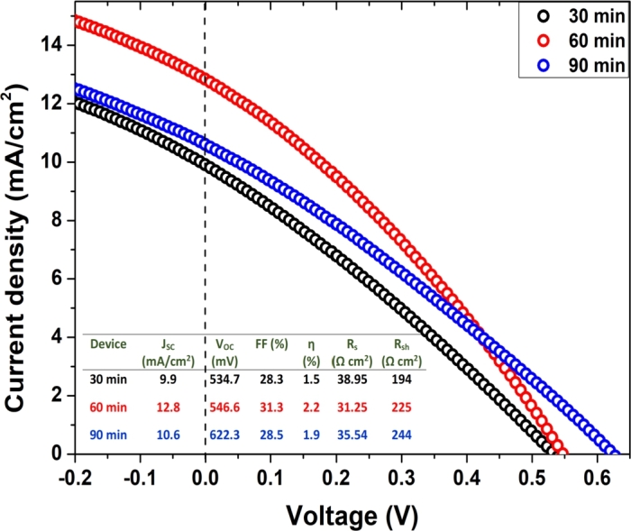
J-V characteristics of the CuSbS2 thin film solar cells prepared at 430 oC for 30–90 min.
4. Conclusions
Highly crystalline phase-pure CuSbS2 thin films were developed by sulfurizing thermally evaporated Cu/Sb/Cu stacks at 400 and 430 oC for different durations. Films sulfurized at 400 oC showed orthorhombic CuSbS2 as the dominant phase with Sb2S3 as the secondary phase for 10–60 min, and Cu3SbS4 phase at 90 min duration. The average particle size of the films increased from 0.5 to 1.5 μm with an increase in sulfurization time from 10 to 60 min and decreased to 1.0 μm at 90 min. The electrical resistivity decreased, and the carrier concentration increased with an increase in sulfurization time at 400 oC. The films developed at 430 oC demonstrated a Cu3SbS4 secondary phase after 10 min and phase-pure CuSbS2 after 30 min of sulfurization. The average particle size of the films increased from 1.5 to 2 μm with an increased sulfurization time. The direct optical bandgap of CuSbS2 was found to be 1.41 eV. The electrical resistivity decreased, and the carrier concentration increased with increased sulfurization time at 430 oC. Based on this study, it can be concluded that large-grained single-phase CuSbS2 films can be fabricated by sulfurizing the Cu/Sb/Cu stacks at 430 oC for 30–90 min. Fabrication of CuSbS2 solar cells using an absorber prepared at 430 oC for 30 min resulted in an efficiency of 1.5% with a J of 9.9 mA/cm2, V of 534.7 mV, and FF of 28.3%. An increase in the sulfurization time to 60 min resulted in an increase in the device efficiency to 2.2% with a J of 12.8 mA/cm2, V of 546.6 mV, and FF of 31.3%. A further increase in the duration to 90 min resulted in a slight decrease in the device efficiency to 1.9% and an increase in V to 622.3 mV.
CRediT authorship contribution statement
U. Chalapathi: Writing – original draft, Software, Methodology, Investigation, Formal analysis, Data curation, Conceptualization. P. Uday Bhaskar: Visualization, Validation, Investigation, Formal analysis. Sambasivam Sangaraju: Visualization, Methodology, Formal analysis. Bandar Ali Al-Asbahi: Visualization, Formal analysis. Si-Hyun Park: Writing – review & editing, Supervision, Resources, Project administration, Funding acquisition.
Declaration of Competing Interest
The authors declare that they have no known competing financial interests or personal relationships that could have appeared to influence the work reported in this paper.
Acknowledgements
This research was supported by Regional Innovation Strategy (RIS) through the National Research Foundation of Korea (NRF) funded by the Ministry of Education (MOE) (No. 2022RIS-006).
Data availability
Data will be made available on request.
References
- 1.Yoshikawa K., Kawasaki H., Yoshida W., Irie T., Konishi K., Nakano K., Uto T., Adachi D., Kanematsu M., Uzu H., Yamamoto K. Silicon heterojunction solar cell with interdigitated back contacts for a photoconversion efficiency over 26% Nat. Energy. 2017;2:1–8. [Google Scholar]
- 2.Wilson G.M., Al-Jassim M., Metzger W.K., Glunz S.W., Verlinden P., Xiong G., Mansfield L.M., Stanbery B.J., Zhu K., Yan Y., et al. The 2020 photovoltaic technologies roadmap. J. Phys. D, Appl. Phys. 2020;53 [Google Scholar]
- 3.Green M., Dunlop E., Hohl-Ebinger J., Yoshita M., Kopidakis N., Hao X. Solar cell efficiency tables (version 57) Prog. Photovolt. 2021;29:3–15. [Google Scholar]
- 4.NREL . 2023. Interactive Best Research-Cell Efficiency Chart. [Google Scholar]
- 5.Umehara M., Tajima S., Aoki Y., Takeda Y., Motohiro T. Cu2SnGexS3 solar cells fabricated with a graded bandgap structure. Appl. Phys. Express. 2016;9 [Google Scholar]
- 6.Sinsermsuksakul P., Sun L., Lee S.W., Park H.H., Kim S.B., Yang C., Gordon R.G. Overcoming efficiency limitations of SnS-based solar cells. Adv. Energy Mater. 2014;4 [Google Scholar]
- 7.Welch A.W., Zawadzki P.P., Lany S., Wolden C.A., Zakutayev A. Self-regulated growth and tunable properties of CuSbS2 solar absorbers. Sol. Energy Mater. Sol. Cells. 2015;132:499–506. [Google Scholar]
- 8.Rabhi A., Kanzari M., Rezig B. Growth and vacuum post-annealing effect on the properties of the new absorber CuSbS2 thin films. Mater. Lett. 2008;62:3576–3578. [Google Scholar]
- 9.Suriakarthick R., Kumar V.N., Shyju T., Gopalakrishnan R. Effect of substrate temperature on copper antimony sulphide thin films from thermal evaporation. J. Alloys Compd. 2015;651:423–433. [Google Scholar]
- 10.Rastogi A., Janardhana N. Properties of CuSbS2 thin films electrodeposited from ionic liquids as p-type absorber for photovoltaic solar cells. Thin Solid Films. 2014;565:285–292. [Google Scholar]
- 11.Choi Y.C., Yeom E.J., Ahn T.K., Seok S.I. CuSbS2-sensitized inorganic–organic heterojunction solar cells fabricated using a metal–thiourea complex solution. Angew. Chem. Int. Ed. 2015;54:4005–4009. doi: 10.1002/anie.201411329. [DOI] [PubMed] [Google Scholar]
- 12.Wang W., Hao L., Zhang W., Lin Q., Zhang X., Tang Z. Preparation of CuSbS2 thin films by a facile and low-cost chemical solution method. J. Mater. Sci., Mater. Electron. 2018;29:4075–4079. [Google Scholar]
- 13.Manolache S., Duta A., Isac L., Nanu M., Goossens A., Schoonman J. The influence of the precursor concentration on CuSbS2 thin films deposited from aqueous solutions. Thin Solid Films. 2007;515:5957–5960. [Google Scholar]
- 14.Macías C., Lugo S., Benítez Á., López I., Kharissov B., Vázquez A., Peña Y. Thin film solar cell based on CuSbS2 absorber prepared by chemical bath deposition (CBD) Mater. Res. Bull. 2017;87:161–166. [Google Scholar]
- 15.Rodriguez-Lazcano Y., Nair M., Nair P. CuxSbySz thin films produced by annealing chemically deposited Sb2S3–CuS thin films. Mod. Phys. Lett. B. 2001;15:667–670. [Google Scholar]
- 16.Vinayakumar V., Shaji S., Avellaneda D., Roy T.D., Castillo G., Martinez J., Krishnan B. CuSbS2 thin films by rapid thermal processing of Sb2S3-Cu stack layers for photovoltaic application. Sol. Energy Mater. Sol. Cells. 2017;164:19–27. [Google Scholar]
- 17.Septina W., Ikeda S., Iga Y., Harada T., Matsumura M. Thin film solar cell based on CuSbS2 absorber fabricated from an electrochemically deposited metal stack. Thin Solid Films. 2014;550:700–704. [Google Scholar]
- 18.Banu S., Ahn S.J., Ahn S.K., Yoon K., Cho A. Fabrication and characterization of cost-efficient CuSbS2 thin film solar cells using hybrid inks. Sol. Energy Mater. Sol. Cells. 2016;151:14–23. [Google Scholar]
- 19.Sadanand, Dwivedi D. Modeling of photovoltaic solar cell based on CuSbS2 absorber for the enhancement of performance. IEEE Trans. Electron Devices. 2021;68:1121–1128. [Google Scholar]
- 20.Wang W., Winkler M.T., Gunawan O., Gokmen T., Todorov T.K., Zhu Y., Mitzi D.B. Device characteristics of CZTSSe thin-film solar cells with 12.6% efficiency. Adv. Energy Mater. 2014;4 [Google Scholar]
- 21.Chalapathi U., Poornaprakash B., Ahn C.-H., Park S.-H. Two-stage processed CuSbS2 thin films for photovoltaics: effect of Cu/Sb ratio. Ceram. Int. 2018;44:14844–14849. [Google Scholar]
- 22.Colombara D., Peter L.M., Rogers K.D., Painter J.D., Roncallo S. Formation of CuSbS2 and CuSbSe2 thin films via chalcogenisation of Sb–Cu metal precursors. Thin Solid Films. 2011;519:7438–7443. [Google Scholar]
- 23.Wan L., Ma C., Hu K., Zhou R., Mao X., Pan S., Wong L.H., Xu J. Two-stage co-evaporated CuSbS2 thin films for solar cells. J. Alloys Compd. 2016;680:182–190. [Google Scholar]
- 24.Chalapathi U., Bhaskar P.U., Cheruku R., Sambasivam S., Park S.-H. Evolution of large-grained CuSbS2 thin films by rapid sulfurization of evaporated Cu–Sb precursor stacks for photovoltaics application. Ceram. Int. 2023;49:4758–4763. [Google Scholar]
- 25.Zhang Y., Huang J., Yan C., Sun K., Cui X., Liu F., Liu Z., Zhang X., Liu X., Stride J.A., Green M.A., Hao X. High open-circuit voltage CuSbS2 solar cells achieved through the formation of epitaxial growth of CdS/CuSbS2 hetero-interface by post-annealing treatment. Prog. Photovolt. 2019;27:37–43. [Google Scholar]
- 26.Norton M.G., Suryanarayana C. Plenum Press; 1998. X-Ray Diffraction: A Practical Approach. [Google Scholar]
- 27.Baker J., Kumar R.S., Sneed D., Connolly A., Zhang Y., Velisavljevic N., Paladugu J., Pravica M., Chen C., Cornelius A., et al. Pressure induced structural transitions in CuSbS2 and CuSbSe2 thermoelectric compounds. J. Alloys Compd. 2015;643:186–194. [Google Scholar]
- 28.Fu L., Yu J., Wang J., Xie F., Yao S., Zhang Y., Cheng J., Li L. Thin film solar cells based on ag-substituted CuSbS2 absorber. Chem. Eng. J. 2020;400 [Google Scholar]
- 29.Rodrıguez-Lazcano Y., Nair M., Nair P. CuSbS2 thin film formed through annealing chemically deposited Sb2S3–CuS thin films. J. Cryst. Growth. 2001;223:399–406. [Google Scholar]
- 30.Ornelas-Acosta R., Avellaneda D., Shaji S., Castillo G., Roy T.D., Krishnan B. CuSbS2 thin films by heating Sb2S3/Cu layers for PV applications. J. Mater. Sci., Mater. Electron. 2014;25:4356–4362. [Google Scholar]
- 31.Chalapathi U., Poornaprakash B., Park S.-H. Growth and properties of Cu3SbS4 thin films prepared by a two-stage process for solar cell applications. Ceram. Int. 2017;43:5229–5235. [Google Scholar]
- 32.Chalapathi U., Poornaprakash B., Cui H., Park S.-H. Two-stage processed high-quality famatinite thin films for photovoltaics. Superlattices Microstruct. 2017;111:188–193. [Google Scholar]
- 33.Morales A.E., Mora E.S., Pal U. Use of diffuse reflectance spectroscopy for optical characterization of un-supported nanostructures. Rev. Mex. Fis. 2007;53:18–22. [Google Scholar]
- 34.Bhaskarand P.U., Dhage S.R. CdS buffer layer by CBD on 300 mm x 300 mm glass for CIGS solar cell application. Mater. Today Proc. 2017;4:12525–12528. [Google Scholar]
- 35.Rabhi A., Kanzari M., Rezig B. Optical and structural properties of CuSbS2 thin films grown by thermal evaporation method. Thin Solid Films. 2009;517:2477–2480. [Google Scholar]
- 36.Welch A.W., Baranowski L.L., Zawadzki P., DeHart C., Johnston S., Lany S., Wolden C.A., Zakutayev A. Accelerated development of CuSbS2 thin film photovoltaic device prototypes. Prog. Photovolt. 2016;24:929–939. [Google Scholar]
Associated Data
This section collects any data citations, data availability statements, or supplementary materials included in this article.
Data Availability Statement
Data will be made available on request.