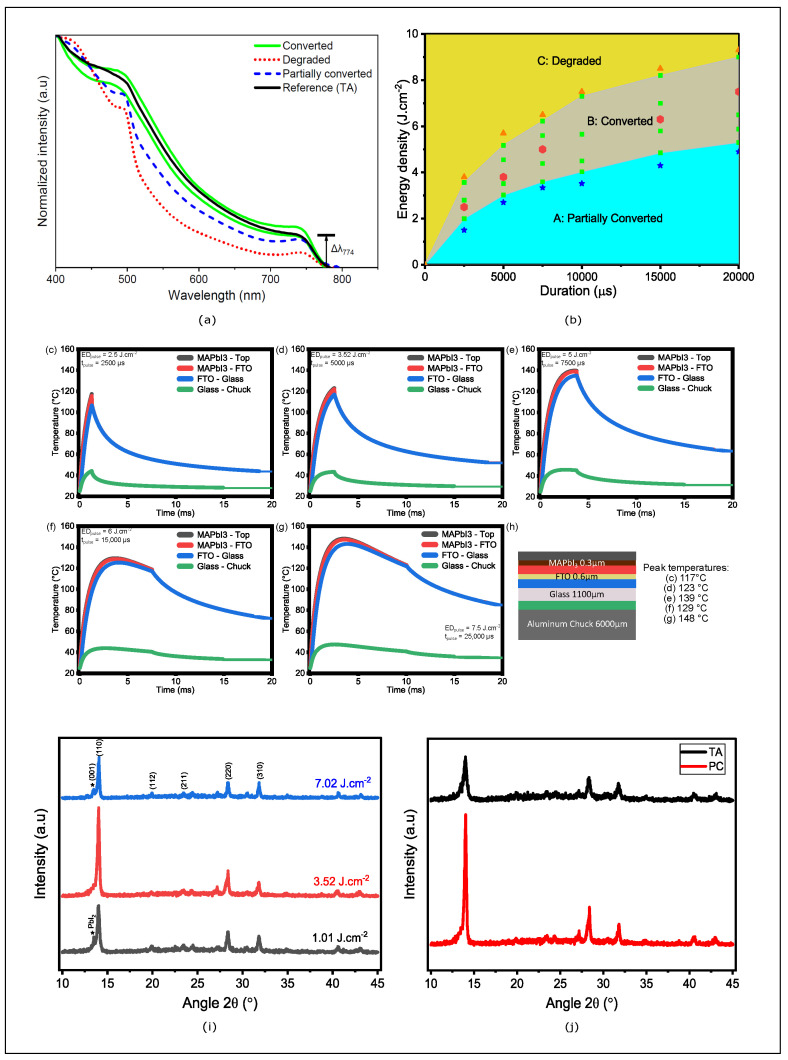
Figure 2.
(a) Absorbance spectra of TA MAPI films (black line) partially converted PC (dashed blue line) when of the PC is below 90% of the TA reference (low energy density), converted PC (green line) when of the PC is superior to 90% (medium energy density), and degraded PC (dashed red line) when is inferior to 90% (high energy density). (b) Mapping of photonically annealed perovskite films based on criterion (a), partially converted (turquoise zone), fully converted (gray zone), and degraded (yellow zone). SimPulse simulations of MAPI film temperature profiles at pulse lengths and density energies corresponding to the center of the conversion zone (red hexagon); (c) 2.5 J·cm−2/2500 ; (d) 3.52 J·cm−2/5000 ; (e) 5 J·cm−2/7500 ; (f) 6 J·cm−2/15,000 ; (g) 7.5 J·cm−2/20,000 . (h) The configuration used for the temperature simulation, and the maximum temperature for each photonic annealing. (i) XRD patterns of MAPI films deposited on a glass substrate and photonically annealed at 5000 pulse duration and energy densities of 1.01 J·cm−2 (black line), 3.52 J·cm−2 (red line), and 7.02 J·cm−2 (blue line), * corresponds to the diffraction of the peak associated with the (001) plane. (j) XRD patterns for the MAPI films, the thermally annealed reference film (black line), and the photonically annealed film at 5000 and 3.52 J·cm−2 (red line).

