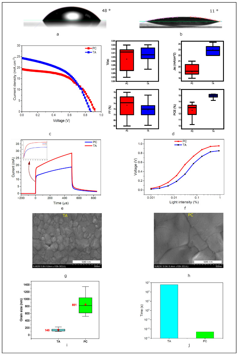
Figure 4.
Contact angle measurement of the ink droplet on the coated substrate, (a) before plasma treatment and (b) after plasma treatment. (c) Device performance of champion of TA and PC, (d) Statistical distribution of the photovoltaic parameters for photonically and thermally annealed perovskite solar cells. (e) Transient photocurrent of the champion devices of TA and PC. (f) Open circuit voltage vs. light intensity of TA and PC champion devices. (g,h) SEM images of thermally and photonically annealed perovskite films. (i) Grain size distribution of thermally and photonically annealed perovskite films. (j) Comparison of the processing time for PC and TA.

