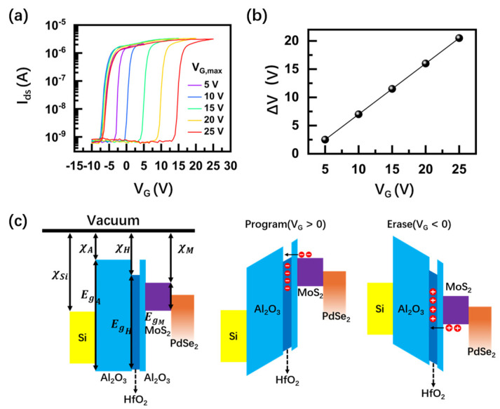
Figure 2.
The statical behavior of the nonvolatile gate charge-trap memory based on MoS2/PdSe2 heterostructure: (a) Ids–VG characteristics of the device under different VG at Vds = −1 V; (b) extraction of memory window ∆V vs. VG. The memory window increases from 1 to ∼20 V in our experimental settings; (c) band diagram of the program/erase state of the device under positive and negative VG. Positive VG programs the device. Electrons tunneling from the few-layer MoS2 channel are accumulated in the HfO2 charge-trap layer. Negative VG erases the device. Holes tunnel from the few-layer MoS2 channel to the HfO2 charge-trap layer.

