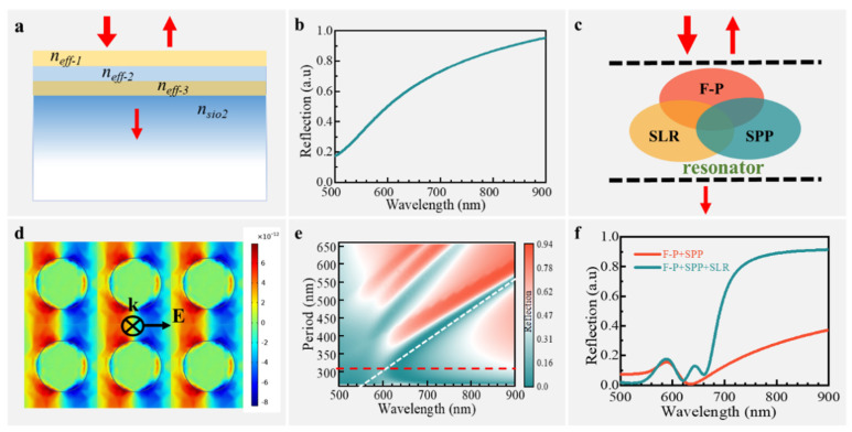
Figure 3.
Formation mechanism of double Fano resonance in the proposed SERS chip. (a) The SERS chip with a subwavelength period is equivalent to a 3-layer thin film system under equivalent medium theory; (b) F-P resonance-like reflectance spectra in the equivalent 3-layer thin film system; (c) schematic diagram of the three resonance modes (F-P-like, slr, and SPP-Bloch) supported simultaneously in the SERS chip and their interactions; (d) the surface charge distribution of the SPP-Bloch resonance formation calculated by FEM simulation, where k represents the incident light wave vector and E represents the direction of electric field polarization; (e) reflectance spectra of SPP-Bloch mode with different nanopore periods coupling to the F-P mode, where the red curve represents the reflection spectrum with a nanohole period p = 315 nm; and (f) comparison of reflectance spectra in SERS chip when there is interaction between only two resonance modes (SPP-Bloch and F-P) and three resonance modes (SPP-Bloch, SLR, and F-P).

