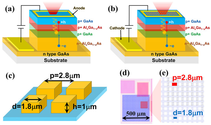
Figure 1.
(a) The optimized LED device with a conversional planar structure. (b) The optimized LED with surface microstructure. (c) The detailed parameters of the micro mesas. (d) schematic diagram of the mask of the entire device. (e) A local pattern of the mask was used for surface microstructure preparation.

