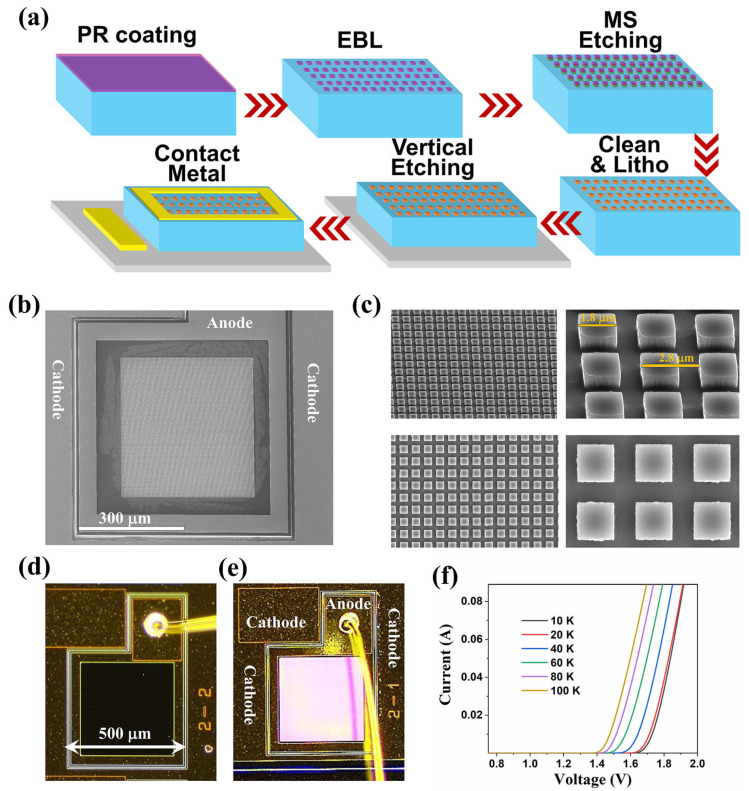
Figure 2.
(a) The device preparation process flow, in which the arrow points represent the flow order. (b) The scanning electron microscope (SEM) image of the prepared microstructure device. (c) Magnified SEM image of the prepared microstructure device. (d) Optical microscope photograph of the prepared planar device without any microstructure. (e) Optical microscope photograph of the prepared device with microstructures. (f) I–V curves of the device at different temperatures.

