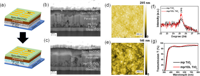
Figure 2.
Structure and characterization of PSCs tested herein. (a) Schematic diagram of the device structure before (top) and after (bottom) introduction of 1DL as an interfacial layer. (b) Cross-sectional SEM image of PSCs before (top panel) 1DL layer deposition. (c) Cross-sectional SEM image of PSCs after the deposition of the 1DL layer on mp TiO2 (bottom panel). (d) AFM map of mp TiO2 and (e) AFM map of mp/1DL TiO2 layers on ITO. (f) XRD patterns of mp TiO2 (bottom black curve) and mp/1DL TiO2 layers (top red curve). (g) Transmission spectra of mp and mp/1DL TiO2 films (black and red curves, respectively).

