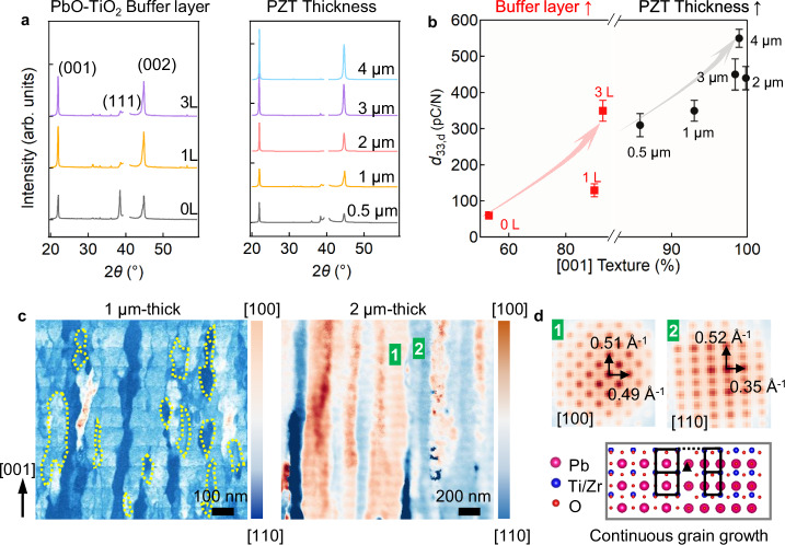
Fig. 2. Structural characterization of textured Pb(Zr,Ti)O3 (PZT) films.
a The plot of theta-omega XRD scan for 1 μm film with different numbers of buffer layers, and for films with different thicknesses on 3 buffer layers. b Macroscopic d33,d as a function of texture degree, which is optimized through the numbers of buffer layer and film thicknesses. The error bars originate from multiple samples. c Grain mapping by diffraction under nanobeam mode across the film with brightly contrasting stripe patterns penetrating the 1 μm (left) and 2 μm-thick (right) PZT films. The color scale bars represent in-plane grain orientation, which may vary from sample to sample depending on the regions outside the 4-inch film. d Nano-diffraction patterns of adjacent [100] and [110] grains (above), the schematic illustration of the twisted grains (bottom), demonstrating the interfacial structure across the twisted boundaries.

