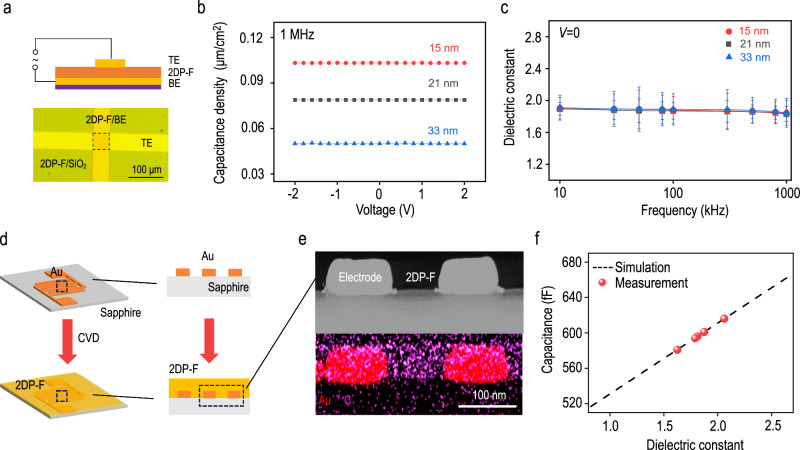
Fig. 2. Dielectric properties of 2DP-F films.
a Schematic illustration of the structure (top) and optical image (bottom) of the parallel plate capacitor. 2DP-F film was directly grown on bottom electrode (BE) and top electrodes (TE) were transferred on top of the film. b Voltage-dependent capacitance (C–V) and (c) Relative dielectric constant as a function of frequency (C–f) for parallel plate capacitors of 2DP-F thin films with varied thicknesses. The error bars were based on five devices for each thickness. d schematic illustration of 2DP-F thin films grown in the gaps of interdigitated capacitors. The Right figure illustrates the cross-section of interdigitated capacitors in the dashed square. e Transmition electron microscope (TEM) image (top) and the energy dispersive X-ray spectroscopy (EDS) elemental mapping of the cross-section of the interdigitated capacitors. f Dielectric constant determination from the Silvaco TCAD simulation. The black dashed line corresponds to the dielectric constant of the interdigitated capacitors as a function of the dielectric constant of the gap-filling materials. Red dots correspond to the measured capacitance of the capacitors after filling the gaps with 2DP-F materials. Inset is a modeled equivalent circuit of impedance behavior in the interdigitated capacitors.

