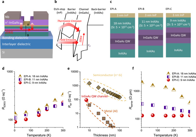
Fig. 2. Design of III–V heterostructure for cryogenic devices.
a Schematic of the III–V heterostructure on Si with Al2O3 bonding dielectric and SiO2 interlayer dielectric. b Illustration of the conduction band of III–V heterostructure along the line AB in (a). Two different emission mechanisms (thermionic emission and field emission) are shown. At cryogenic temperatures, field emission is a dominant mechanism. c Three different III–V heterostructures with different barrier thicknesses. The InAlAs barrier thicknesses are 18, 11, and 9 nm, respectively, and all other layers are the same. d R2DEG versus temperature for three different III-V heterostructures. e Rsh versus thickness at 4 K for III–V 2DEG and conventional metal (Al) and semiconductor (n+-Si). Rsh of III–V 2DEG is more than 10 times lower than typical high-doped Si and comparable to Al metal of the same thickness. f Dependence of Rbarrier on temperature in different III–V heterostructure. As the temperature decreases, the difference in the Rbarrier attributable to variations in barrier thickness increases. This phenomenon is caused by a change in the mechanism at cryogenic temperatures and underscores the crucial role of barrier scaling at cryogenic temperatures.

