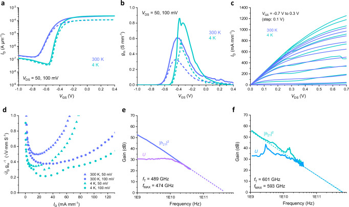
Fig. 3. Electrical performance of cryogenic III-V HEMT on Si for low noise amplifier.
Transfer (a) and transconductance (b) characteristics of III–V HEMTs on Si with LG of 70 nm and WG of 2 × 20 μm measured at VDS of 50 (dashed) and 100 mV (solid). The measurements were conducted at 300 K and 4 K. When cooled to 4 K, the device exhibits transfer characteristics with improved SS of 35 mV dec−1 at VDS = 50 mV. The positive threshold voltage (VTH) shift is also observed. The device offers sharper gm characteristics and a high peak gm of 0.8 S mm−1 at 4 K for a low VDS of 100 mV, compared to those observed at 300 K. This improvement at 4 K is attributed to enhanced 2DEG mobility and a reduction in parasitic resistance. c Output characteristics of the same device, showing improved on-resistance and increased maximum current at 4 K. d Noise indication factor versus ID of the device at a low VDS of 50 and 100 mV. The measurements were conducted at 300 K and 4 K. The device shows a very low noise indication factor of 0.21 and the PDC at minimum noise indication factor is only 0.8 and 2 mW mm−1 at VDS = 50 and 100 mV. Gain plots of III–V HEMTs on Si with LG of 70 nm and WG of 2 × 20 μm measured at 300 K (e) and 4 K (f). The measurements were conducted at VDS of 500 mV and the optimal VGS for each temperature. The fT and fMAX are extracted by extrapolating the h21 and U curves with −20 dB dec−1 lines.

