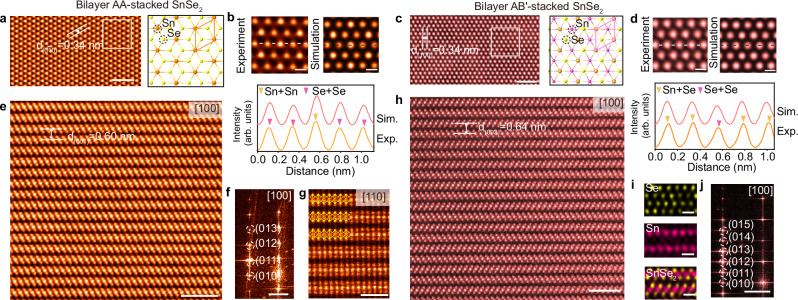
Fig. 2. Atomic-resolution images of AA- and AB′-stacked SnSe2.
a Annular dark field scanning transmission electron microscopy (ADF-STEM) image of AA-stacked SnSe2 along the [001] direction. The corresponding atomic model was depicted on the right panel. b Enlarged ADF image from a with simulated image calculated from AA-stacked SnSe2. Intensity line profiles derived from the experiment and simulation were shown in the lower panel. c ADF-STEM image of AB′-stacked SnSe2 along the [001] direction. The atomic model was depicted on the right panel. d Enlarged ADF image from c and corresponding simulated image derived from AB′-stacked SnSe2. Intensity line profiles extracted from the experiment and simulation were depicted in the lower panel. e Cross-sectional ADF-STEM image of AA-stacked SnSe2 along the [100] zone axis and f its corresponding fast Fourier transformation (FFT) pattern. g Cross-sectional ADF-STEM image of AA-stacked SnSe2 along the zone axis. h ADF-STEM image of AB′-stacked SnSe2 along the [100] direction. i Corresponding EDS mapping showing Se, Sn, and overlaid image. j The FFT pattern derived from h. Scale bars: a, c 1 nm, b, d 0.2 nm; e, h 2 nm; f, j 2 nm−1; g 1 nm; i 0.5 nm.

