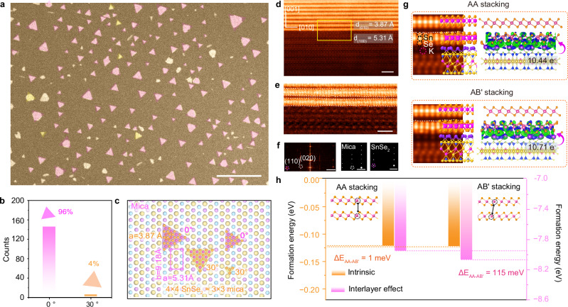
Fig. 3. Underlying mechanisms for growing SnSe2 with novel phases.
a Scanning electron microscopy (SEM) image showing epitaxial growth of SnSe2 flakes on mica substrate. b The statistical counting shows the distribution of 0° and 30° twisted SnSe2 flakes grown on mica. c Schematic illustration depicting SnSe2 flakes grown on mica substrate with different crystallographic orientations. d The atomic-resolution cross-sectional ADF-STEM image of AB′-stacked SnSe2/mica substrate along the zone axis. e The zoom-in ADF-STEM image reveals atomic distortion as depicted by the white dashed lines along the interface. f Corresponding FFT pattern from (e). Simulated FFT patterns of mica and AB′-stacking SnSe2 were shown on the right panels. g The simulated ADF-STEM images derived from the density functional theory (DFT)-optimized AA- and AB′-stacked SnSe2 on the mica surface. The right panel showing the differential charge density of AA-, and AB′-stacked SnSe2 on mica substrate. The area in green is the region that gained electrons, and the area in blue is the region that lost electrons. h DFT calculated formation energies of AA-stacked SnSe2 and AB′-stacked SnSe2 before and after considering the interface effect, respectively. ΔEAA-AB′ denotes the difference in formation energy. The orange dashed line represents the formation energy of AA stacking, while the pink dashed line represents the formation energy of AB′ stacking, both represent with and without the influence of the mica substrate, respectively. Scale bars: a 10 μm; b, e 1 nm; f 2 nm−1.

