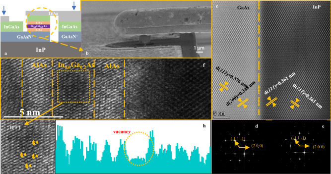
Fig. 2. NDR memristor device analysis.
a Device structure diagram, the yellow circle part is the quantum well (QW) structure. b SEM image of “air bridge” structure. c High-angle annular dark field scanning TEM image of InP and GaAs structure. d, e corresponding to the fast Fourier transform of GaAs and InP, respectively. f High resolution TEM image of QW structure in (a). g In the inverse FFT image of In0.8Ga0.2As, it can clearly see the defects marked in the yellow circle. h Line profiles of the areas with and without atomic vacancies in In0.8Ga0.2As.

