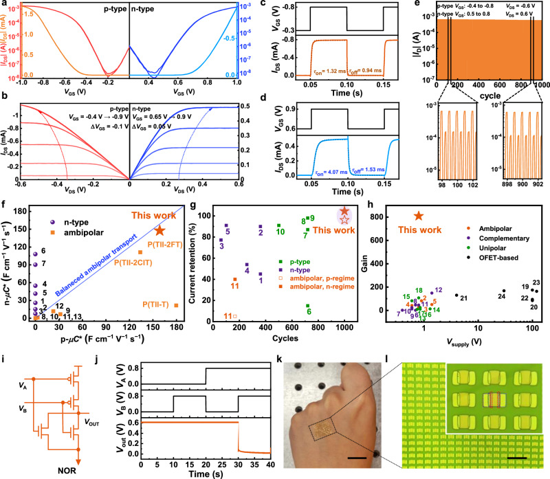
Fig. 4. OECT device and logic circuits fabrication and characterization.
a Transfer and b output characteristics based on P(TII-2FT) (W/L = 100/10 µm). Transient response behavior of the c p-type and d n-type working regime of P(TII-2FT). e Operational stability over 1000 on-off cycling and alternating polarities of the OECT device. f Performance and g device stability comparison of our polymers with some state-of-the-art p-type, n-type, and ambipolar OECT materials (Supplementary Tables 5 and 6). h Comparison of the gain and supply voltage of the different types of inverters (Supplementary Table 7). i Circuit diagram and j voltage input and output behavior given by the NOR gate based on P(TII-2FT). k A flexible transistor array with 300 × 300 inverters attached to the back of a hand (scale bar: 1 cm). l Microscope image of the inverter array. Inset: enlarged microscope image of the inverter array (blue dashed line: VDD electrode contour; purple dashed line: VSS or VGND electrode contour; green dashed line: VOUT electrode contour; red dashed line: ambipolar OECT material channel contour; scale bar: 100 μm).

