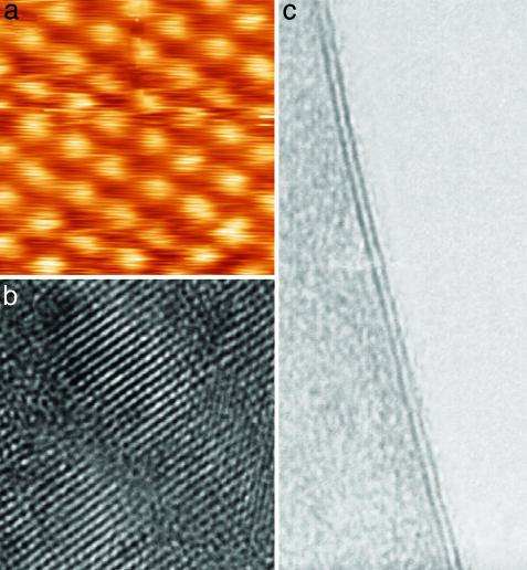
Fig. 2.
Atomic-resolution images of 2D materials. (a) Unfiltered scanning tunneling microscopy image of the crystal lattice in the NbSe2 monolayer on top of an oxidized Si wafer. Note that for the scanning tunneling microscopy measurements, an Au film was deposited around 2D crystallites to provide an electrical contact. (b) HRTEM images of the 2D Bi2Sr2CaCu2Ox crystal shown in Fig. 1c. (c) HRTEM image of a double-layer MoS2. This image is shown to make a connection between our approach based on AFM identification of 2D crystals and the traditional HRTEM approach used for quasi-1D crystals (all nanotubes were first found by using HRTEM, where dark lines indicating the nanotube's walls parallel to the electron beam are easily visible). No similar signature exists for 2D crystals (see refs. 6-8), and we also found it difficult to align 2D samples exactly parallel to the electron beam. However, for two-layer crystals, their thickness is easily identifiable not only in AFM but also in HRTEM because of folded regions seen as two dark lines (in the case of c, the separation is ≈6.5 Å, in agreement with the interlayer distance in bulk MoS2). We occasionally observed short dark lines (compare with ref. 8) that might be folded monolayers, but no independent proof for this (e.g., by simultaneous AFM studies) has been obtained yet.

