

Abstract
Fingerprint‐on‐display (FoD) sensors utilizing organic photodetectors (OPDs) are nearing commercialization, making it crucial to develop novel conjugated polymers that can be used as the active layer for this technology. These polymers should meet several requirements in terms of patent rights, large‐scale synthesis, and OPD performance. In this study, novel conjugated polymers containing electron‐withdrawing building blocks, easily synthesized from a 2‐aminothiazole‐4‐carboxylate Schiff base commonly used as a pharmaceutical intermediate, are developed for high‐performance OPDs and FoD sensors. Through alkyl chain engineering of the synthesized polymers, the highest photocurrent density and the lowest dark current density values were achieved in the OPDs. This resulted in the best OPD performance with a promising responsivity of 0.42 A/W and specific detectivity of 2.6 × 10¹³ Jones at −2 V under near‐infrared irradiation (810 nm). In addition, they exhibited excellent performance with a rising response time of 3–4 µs, falling response time of 6–11 µs, and −3 dB cut‐off frequency of 80–100 kHz. Finally, the OPD is integrated into an organic thin‐film transistor array to build a FoD sensor with 80 × 80 µm2 pixels, resulting in the successful acquisition of a digital fingerprint image.
Keywords: 2‐aminothiazole‐4‐carboxylate Schiff base, conjugated polymer, fingerprint‐on‐display sensor, high specific detectivity, organic photodetector
Four novel conjugated polymers are developed for high‐performance organic photodetectors (OPDs) and fingerprint‐on‐display sensors. Optimization of alkyl side‐chains achieved promising responsivity of 0.42 A/W and specific detectivity of 2.6 × 10¹3 Jones at −2 V under near‐infrared light. The OPD is integrated into an organic thin‐film transistor array, successfully capturing a digital fingerprint image with 80 × 80 µm2 pixels.

1. Introduction
Finding new conjugated building blocks is crucial for diversifying conjugated polymers and realizing novel optoelectronic properties.[ 1 , 2 , 3 , 4 , 5 , 6 ] Fundamentally, these building blocks must be fully conjugated and have functional groups capable of substituting alkyl chains to produce solution‐processable polymers.[ 7 , 8 , 9 ] Currently, a variety of widely used conjugated building blocks, such as benzodithiophene, fluorene, diketopyrrolopyrroles, and thienopyrroledione, meet these two requirements.[ 10 , 11 , 12 , 13 , 14 ] We found that 2‐aminothiazole‐4‐carboxylate Schiff base, which is commonly used as a pharmaceutical intermediate, has significant potential as a new building block for conjugated polymers.[ 15 , 16 ] This Schiff base is easily synthesized with quantitative yields through a heterocyclic aromatic ring formation reaction between β‐bromopyruvic acid ethyl ester and thiourea, making it very promising for mass production.[ 17 , 18 ] In addition, a simple transesterification reaction allows for the facile introduction of various alkyl chains to the Schiff base.[ 19 ] However, research on the development of conjugated backbones based on this Schiff base has rarely been reported. Therefore, this study aims to develop novel conjugated polymers from this Schiff base that are suitable for applications in high‐performance organic photodetectors (OPDs) and fingerprint‐on‐display (FoD) sensors.
Recently, OPDs have received considerable attention owing to their promising roles in cutting‐edge flexible technologies, including optical communication systems, high‐resolution CMOS sensors, portable X‐ray detectors, FoD sensors, and wearable health monitoring systems.[ 20 , 21 , 22 , 23 , 24 , 25 , 26 , 27 , 28 , 29 , 30 , 31 ] For the successful development of such OPD‐related sensors, the most crucial prerequisite layer is a photoactive layer composed of polymer donors and electron acceptors. This active layer should exhibit a high photocurrent density (J ph) and low dark current density (J d), along with fast dynamic characteristics.[ 32 , 33 , 34 , 35 ] Additionally, a panchromatic absorption of the active layer covering the entire visible and NIR spectra will enable the sensor to detect light across a wide range of wavelengths.[ 36 , 37 ]
To satisfy these requirements, novel electron‐withdrawing building blocks of alkyl 2,5‐bis(5‐bromothiophen‐2‐yl)thiazole‐4‐carboxylate (TTzCs) were first synthesized in five steps starting from β‐bromopyruvic acid ethyl ester. As shown in Scheme 1 , TTzCs are fully conjugated and can easily incorporate various types of alkyl groups through the pendant carboxyl group. Additionally, because of their electron‐withdrawing thiazole and carboxyl groups, they exhibit n‐type characteristics, making TTzCs favorable for the formation of donor‐acceptor (D‐A) structures in conjugated polymers through copolymerization with electron‐donating conjugated building blocks. Moreover, side‐chain engineering of the TTzC building block was systematically performed by increasing the size of the alkyl chains in the order of 2‐butyloctyl (C12H25) < 2‐octyldodecyl (C20H41) < 2‐decyltetradecyl (C24H49) < 2‐dodecylhexadecyl (C28H57), which is important for optimizing the charge transport properties of the conjugated backbone and the insulating properties of the pendant groups. Second, these TTzC monomers were successfully copolymerized with a benzo[1,2‐b:4,5‐b']dithiophene‐based electron‐donating building block, and the corresponding polymers were named PBTTzC1, PBTTzC2, PBTTzC3, and PBTTzC4, respectively. All four PBTTzCx (x = 1, 2, 3, and 4) polymers showed strong green light absorption in the 400–600 nm range; thus, they were blended with a low‐bandgap non‐fullerene acceptor, Y6, to build panchromatic bulk heterojunction (BHJ)‐type OPDs. Finally, all of the fabricated BHJ‐type PBTTzCx:Y6 devices exhibited a panchromatic external quantum efficiency (EQE) in the 400–900 nm range, covering the entire visible and NIR regions. Owing to the strong light detection in the NIR region, the J‐V characteristics of the OPDs were evaluated under NIR light irradiation at 810 nm. Although all of the polymers had identical conjugated backbones, the alkyl side chains significantly affected both the J d and J ph values of the devices. As the alkyl side chains lengthened, they enhanced the intermolecular ordering of the polymers while effectively suppressing the J d values in the devices. However, when the alkyl side chains became excessively long, the morphology of the active layer deteriorated, resulting in decreased OPD performance. Thus, PBTTzC3 containing 2‐decyltetradecyl side chains showed the highest J ph and lowest J d values in the devices. This resulted in the best OPD performance with a promising responsivity (R) of 0.42 A/W and specific detectivity (D*) of 2.6 × 10¹³ Jones at −2 V. Regarding the dynamic characteristics, all of the devices exhibited excellent performance with a rising response time (t r) of 3–4 µs, a falling response time (t f) of 6–11 µs, and a −3 dB cut‐off frequency (f −3 dB) of 80–100 kHz.
Scheme 1.

Synthetic route of TTzCx (x = 1, 2, 3, and 4) and the corresponding polymers.
Considering the highest R and D* values of PBTTzC3:Y6 devices with excellent J d saturation behavior under negative bias, the PBTTzC3:Y6‐based OPD was integrated into an organic thin‐film transistor (OTFT) array to build an FoD sensor with 80 × 80 µm2 pixels. The contrast between the valleys and ridges in the fingerprints was captured as a digital signal, resulting in the successful acquisition of a digital fingerprint image. This study demonstrated that the new TTzC building block, derived from pharmaceutical intermediates that are easily synthesizable from chemicals abundant in nature, is a highly promising structure for constructing high‐performance OPD polymers.
2. Results and Discussion
2.1. Material Characterization
Compound 1 was synthesized with a quantitative yield through a heterocyclic aromatic ring formation reaction between thiourea and ethyl 3‐bromopyruvate. Compound 2 was obtained through bromination of compound 1 using copper (II) bromide. The transesterification reaction between compound 2 and various branched alkyl alcohol sources (2‐butyloctyl alcohol, 2‐octyldodecyl alcohol, 2‐decyltetradecyl alcohol and 2‐dodecylhexadecyl alcohol) successfully produced the corresponding compound 3a, 3b, 3c, and 3d, respectively. Carboxylated dibromide compounds 3a–d were then reacted with tributyl(thiophen‐2‐yl)stannane via a Stille coupling reaction in the presence of a Pd(PPh3)4 catalyst to obtain compounds 4a–d, respectively. The final monomers 5a–d, referred to as TTzC1‐4, respectively, were obtained through bromination using N‐bromosuccinimide (NBS). The synthesized TTzC1–4 monomers show several unique features. They have a strong electron‐withdrawing core unit (TzC) composed of thiazole and carboxylate, which can effectively induce strong visible light absorption and enhance the intermolecular interactions of the polymers by forming a D‐A structure when copolymerized with electron‐donating units. In addition, various alkyl side chains can easily be attached to structures through a simple transesterification reaction at the carboxylate groups. Moreover, the alkylated TzC core unit can be easily converted from the 2‐aminothiazole‐4‐carboxylate Schiff bases (pharmaceutical intermediates), which is beneficial for mass production.
The final TTzC1–4 monomers with alkyl groups of different lengths were polymerized with a 4,8‐bis(5‐(2‐ethylhexyl)thiophen‐2‐yl)benzo[1,2‐b:4,5‐b’]dithiophene‐2,6‐diyl)bis(trimethylstannane) (BDT) monomer via a Stille coupling reaction to obtain D‐A‐type alternating polymer donors. The synthesized polymers were denoted PBTTzC1–4, respectively. The synthesized polymers were purified through Soxhlet extraction with methanol, acetone, hexane, and chloroform to remove the residual catalyst and oligomeric residues. The final yields of PBTTzC1–4 were 82.8%, 82.8%, 83.8%, and 74%, respectively. The synthesized monomers and polymers were identified using 1H and 13C NMR spectroscopy (Figures S1–S18, Supporting Information). The synthetic route is shown in Scheme 1, and the detailed synthetic procedure is provided in the Experimental Section. The molecular weights of the synthesized polymers were evaluated using gel permeation chromatography (GPC) (Figures S19–S22, Supporting Information). The number‐average molecular weights (M n) of PBTTzC1–4 were 6.6, 57.8, 58.1, and 23.5 kDa, respectively, and the weight‐average molecular weights (M W) were 10.8, 203.8, 417.5, and 78.7 kDa, respectively. The molecular weight of PBTTzC1 was much lower than those of the other polymers because of the limited solubility of the polymer caused by the short alkyl side chains. However, the other synthesized polymers readily dissolved in common organic solvents such as chloroform (CF), toluene, and tetrahydrofuran (THF).
The thermal stabilities of the polymers were characterized using thermogravimetric analysis (TGA) (Figure S23, Supporting Information). The 5%‐weight‐loss temperatures of PBTTzC1–4 were 325, 381, 341, and 337 °C, respectively. The lower molecular weight of PBTTzC1 resulted in some issues with thermal stability, whereas the other polymers with higher molecular weights demonstrated excellent thermal stability. Therefore, the molecular weight of the PBTTzC polymers was important for maintaining high thermal stability.
The UV/Vis absorption spectra of the synthesized polymer donors were measured in both solution and film states (Figure 1a,b). The absorption maxima of PBTTzC1–4 were 512, 529, 525, and 518 nm, respectively, in a diluted CF solution (Figure 1a) and 523, 566, 571, and 529 nm, respectively, in the film states (Figure 1b). In a diluted solution, all the polymers exhibited similarly good solubility, indicating that there were no significant intermolecular interactions or aggregation. PBTTzC1 showed the most blue‐shifted absorption and a relatively low absorption coefficient compared with the other polymers. This strongly implies that PBTTzC1 has the weakest intrachain interaction as well as less effective π‐conjugation length compared to the other polymers. The low molecular weight of PBTTzC1 seems to have negatively affected the π‐conjugation of the polymer chain. In contrast, the other polymers exhibited strong green light absorption with sufficient absorption coefficients (Figure S24, Supporting Information). The slight decrease in the maximum absorption intensity from PBTTzC2 to PBTTzC3 to PBTTzC4 was due to the increasing length of the alkyl side chains (Figure S25, Supporting Information). In the film state, the absorption peaks of PBTTzC1–4 were much broader and largely red‐shifted, indicating increased intermolecular interaction of the polymers in the film states. Notably, only PBTTzC2 and PBTTzC3 exhibited clear bimodal absorption peaks. This implies that there was efficient intermolecular π‐π stacking ordering on PBTTzC2 and PBTTzC3, which is beneficial for charge transport in the devices. The short alkyl side chains on PBTTzC1 caused some solubility and π‐conjugation issues, while the overly long alkyl side chains on PBTTzC4 interfered with efficient π‐π stacking in the film states. The optical bandgap of each polymer donor was estimated from the absorption onset wavelength in Figure 1b. Because all of the polymers had the same backbone structure, differing only in the alkyl side chains, they exhibited similar optical bandgaps of 2.0 eV.
Figure 1.
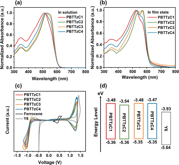
UV/Vis absorption spectra of synthesized polymers in a) solution and b) film state. c) Cyclic voltammetry (CV) plots of synthesized polymers. d) Schematic energy level diagram obtained from the CV plots.
The energy levels of the synthesized polymer donors and Y6 were estimated electrochemically using cyclic voltammetry (CV), as shown in Figure 1c. The highest occupied molecular orbital energy level (EHOMO) and lowest unoccupied molecular orbital energy level (ELUMO) were calculated using the oxidation onset potential (E ox) and reduction onset potential (E re), respectively. The E ox values of PBTTzC1–4 and Y6 were 1.02, 1.02, 1.01, 1.01, and 1.30 V, respectively, which corresponded to E HOMO of −5.36, −5.36, −5.35, −5.35, and −5.64 eV, respectively. Similar to the calculation of E HOMO, the E LUMO values of PBTTzC1‐4 and Y6 were calculated as −3.48, −3.54, −3.48, −3.47, and −3.93 eV, respectively, from E re values of −0.86, −0.81, −0.86, −0.87, and −0.41 V, respectively. All the polymer donors possess suitable HOMO and LUMO energy levels with Y6 acceptor for efficient hole and electron separation and transport in the devices. In addition, as illustrated in Figure 1d, the side chain length did not cause a significant difference in the energy levels of the synthesized polymers. This indicates that the energy levels are not a major factor in determining the OPD characteristics of the synthesized polymers. The optical and electrochemical properties are summarized in Table 1 .
Table 1.
Optical and electrochemical properties of synthesized polymer donors.
| Polymer | Optical Properties | Electrochemical Properties | ||||
|---|---|---|---|---|---|---|
| λmax,sol [nm] a) | λmax,film [nm] b) | Eg opt [eV] c) | Eox/EHOMO [V/eV] d) | Ere/ELUMO [V/eV] e) | Eg CV [eV] f) | |
| PBTTzC1 | 512 | 523 | 2.0 | 1.02/−5.36 | −0.86/−3.48 | 1.88 |
| PBTTzC2 | 529 | 566 | 2.0 | 1.02/−5.36 | −0.81/−3.54 | 1.82 |
| PBTTzC3 | 525 | 571 | 2.0 | 1.01/−5.35 | −0.86/−3.48 | 1.87 |
| PBTTzC4 | 518 | 529 | 2.0 | 1.01/−5.35 | −0.87/−3.47 | 1.88 |
Dilute chloroform solution;
film on a quartz plate formed by spin‐coating chloroform solution;
bandgap calculated from the film‐state absorption onset wavelength, Eg opt = 1240/λonset,film;
HOMO levels determined from Eox by cyclic voltammetry, EHOMO = −[4.8+(Eox−E1/2)] (eV);
ELUMO = Eg opt + EHOMO;
bandgap calculated from the EHOMO and ELUMO levels
2.2. OPD Properties
BHJ‐type OPDs were fabricated with an inverted layer structure of ITO/ZnO‐EDT/Active layer/MoOX/Ag, as illustrated in Figure 2a. To realize panchromatic absorption in the active layer, the PBTTzC1–4 donors, which exhibited strong green light absorption, were blended with the Y6 acceptor, which exhibited strong red NIR absorption (Figure S25, Supporting Information). The thickness of each layer was estimated from the cross‐sectional SEM images as shown in Figure S26 (Supporting Information). The active layers showed slight thickness variations within ≈30 nm under optimal conditions. However, as shown in Figures S27 and S28 (Supporting Information), when the thickness was adjusted to be similar, no significant difference in OPD performance was observed. Details of the device fabrication procedure are presented in the Experimental Section.
Figure 2.

a) Schematic illustration of the fabricated OPD. J‐V curves of b) PBTTzC1:Y6, c) PBTTzC2:Y6, d) PBTTzC3:Y6, and e) PBTTzC4:Y6 using collimated 810 nm LED. f) Noise current spectra of the PBTTzC:Y6 OPDs at a bias of −2.0 V.
The current density–voltage (J‐V) curves of the fabricated OPDs were obtained under 810 nm NIR LED illumination, as shown in Figure 2b–e. The responsivity (R) is defined as the ratio between the photo‐generated current density (Jph ) and the incident light power (Plight ), calculated using Equation (1):[ 38 ]
| (1) |
The calculated R values of the PBTTzC1:Y6, PBTTzC2:Y6, PBTTzC3:Y6, and PBTTzC4:Y6 devices were 0.17, 0.40, 0.42, and 0.39 A/W, respectively, at a bias of −2.0 V, and 0.12, 0.37, 0.41, and 0.36 A/W, respectively, at a bias of −1.0 V under 810 nm LED illumination (≈12 µW cm−2). As the alkyl chain length increased, the R‐value gradually increased. However, when the alkyl group became too long, the R‐value started to decrease. This suggests that as long as the alkyl group is not excessively long, increasing the alkyl chain length not only enhances the solubility of the polymer but also increases the ordering of the polymer through the alignment of the alkyl chains. As a result, the PBTTzC3:Y6 device exhibited a much higher R‐value than the other devices; thus, the 2‐decyltetradecyl side chain appears to be optimal for the PBTTzC backbone structure.
Notably, the alkyl side chains significantly affected the dark current density (J d) of the OPD devices. The J d values of the PBTTzC1:Y6, PBTTzC2:Y6, PBTTzC3:Y6 and PBTTzC4:Y6 devices were 2.09 × 10⁻⁷, 1.13 × 10⁻⁸, 3.65 × 10⁻¹⁰ and 3.23 × 10⁻⁷ A cm−2 at a bias of −2.0 V, respectively, and 5.20 × 10⁻⁹, 5.45 × 10⁻⁹, 1.51 × 10⁻¹, and 2.30 × 10⁻⁸ A cm−2, respectively, at a bias of −1.0 V. The J d values of the devices were significantly suppressed as the alkyl side chains became longer owing to the increased insulating properties of the polymers. However, the decreased J d characteristics of the PBTTzC4:Y6 device with the longest alkyl side chains are speculated to result from suboptimal morphological arrangements between PBTTzC4 and Y6. Increasing the length of the alkyl side chains in the PBTTzC polymers up to the 2‐decyltetradecyl group appears to be a highly effective way to increase J ph while simultaneously decreasing J d in OPDs.
Based on the J ph and J d values of the devices, the shot‐noise‐limited detectivity (D sh*) was calculated using Equation (2), where q is the elementary charge:[ 39 ]
| (2) |
The calculated Dsh* values of the PBTTzC1:Y6, PBTTzC2:Y6, PBTTzC3:Y6, and PBTTzC4:Y6 devices were 6.65 × 10¹¹, 6.63 × 10¹², 3.85 × 10¹³, and 1.23 × 10¹² Jones at −2.0 V, respectively, and 2.94 × 10¹², 8.79 × 10¹², 5.94 × 10¹³, and 4.24 × 10¹² Jones, respectively, at −1.0 V under 810 nm LED illumination (≈12 µW cm−2). The D sh* value of the PBTTzC3:Y6 device was markedly superior to those of the other devices. This can be attributed to two factors: the PBTTzC3:Y6 device had the lowest J d value and highest R‐value.
The specific detectivity (D*) was also evaluated from the noise current density of the devices at −2 V, as shown in Figure 2f. The D* values were calculated using Equation (3), where A is the area of the photoconductive layer, B is the bandwidth, and in is the noise current density.[ 40 , 41 , 42 ]
| (3) |
As shown in Figure 2f, the white noise current (thermal and shot noise current) was dominant in the total noise current, whereas 1/f noise (flicker noise) was observed only at very low frequencies below 10 Hz. The in values of the PBTTzC1:Y6, PBTTzC2:Y6, PBTTzC3:Y6, and PBTTzC4:Y6 devices were 1.02 × 10⁻¹³, 1.96 × 10⁻¹⁴, 4.88 × 10⁻¹⁵, and 9.30 × 10⁻¹⁴ A/Hz0.5, respectively. The PBTTzC3:Y6 device showed the lowest in values, which is consistent with the trend in the J d values observed in the J‐V curves (Figure 2b−e). The corresponding D* values were 5.06 × 10¹¹, 6.11 × 10¹², 2.56 × 10¹³, and 1.27 × 1012 cm Hz0.5/W, respectively, under 810 nm LED illumination (≈12 µW cm−2) at a bias of −2.0 V (Table 2 ). The PBTTzC3:Y6 device exhibited the highest D* among the fabricated devices.
Table 2.
OPD properties of PBTTzCx:Y6 devices under 810 nm LED light of varying intensity at a bias of −2 V.
| Donor:Acceptor | P in [W/cm2] | J d [A/cm2] | J ph [W/cm2] | i noise [A/Hz0.5] | R [A/W] | D sh* [Jones] | D* [Jones] | Bias [V] |
|---|---|---|---|---|---|---|---|---|
| PBTTzC1:Y6 | 1.20 × 10⁻⁵ | 2.09 × 10⁻⁷ | 2.06 × 10⁻⁶ | 1.02 × 10⁻¹³ | 0.172 | 6.65 × 10¹¹ | 5.06 × 10¹¹ | −2 |
| 4.97 × 10⁻³ | 2.09 × 10⁻⁷ | 5.66 × 10⁻⁴ | 1.02 × 10⁻¹³ | 0.114 | 4.41 × 10¹¹ | 3.35 × 10¹¹ | ||
| PBTTzC2:Y6 | 1.20 × 10⁻⁵ | 1.13 × 10⁻⁸ | 4.79 × 10⁻⁶ | 1.96 × 10⁻¹⁴ | 0.399 | 6.63 × 10¹² | 6.11 × 10¹² | |
| 4.97 × 10⁻³ | 1.13 × 10⁻⁸ | 1.68 × 10⁻³ | 1.96 × 10⁻¹⁴ | 0.338 | 5.61 × 10¹² | 5.17 × 10¹² | ||
| PBTTzC3:Y6 | 1.20 × 10⁻⁵ | 3.65 × 10⁻¹⁰ | 5.00 × 10⁻⁶ | 4.88 × 10⁻¹⁵ | 0.416 | 3.85 × 10¹³ | 2.56 × 10¹³ | |
| 4.97 × 10⁻³ | 3.65 × 10⁻¹⁰ | 1.82 × 10⁻³ | 4.88 × 10⁻¹⁵ | 0.366 | 3.39 × 10¹³ | 2.25 × 10¹³ | ||
| PBTTzC4:Y6 | 1.20 × 10⁻⁵ | 3.23 × 10⁻⁷ | 5.13 × 10⁻⁶ | 9.30 × 10⁻¹⁴ | 0.394 | 1.23 × 10¹² | 1.27 × 10¹² | |
| 4.97 × 10⁻³ | 3.23 × 10⁻⁷ | 1.79 × 10⁻³ | 9.30 × 10⁻¹⁴ | 0.360 | 1.12 × 10¹² | 1.16 × 10¹² |
The noise equivalent power (NEP) is the minimum light power required to detect an electrical signal.[ 43 ] The calculated NEP values for the PBTTzC1:Y6, PBTTzC2:Y6, PBTTzC3:Y6, and PBTTzC4:Y6 devices were 5.93 × 10⁻¹³, 4.91 × 10⁻¹⁴, 1.17 × 10⁻¹⁴, and 2.39 × 10⁻¹³ W/Hz0.5, respectively, at −2 V. The lower the NEP value, the more sensitive the OPDs will be to detecting weaker light signals. Therefore, it can be concluded that the PBTTzC3:Y6 device exhibited the highest sensitivity among the fabricated OPDs, which is attributed to its highest R values and lowest J d values.
The linear dynamic range (LDR) values of the fabricated devices were calculated using Equation (4), where Jmax and Jmin are the maximum and minimum J ph values, respectively, which are linearly related to the incident light power.[ 44 ]
| (4) |
As shown in Figure S32 (Supporting Information), the calculated LDR values of the PBTTzC1:Y6, PBTTzC2:Y6, PBTTzC3:Y6, and PBTTzC4:Y6 devices were 91, 127, 158, and 99 dB, respectively, at a bias of −2.0 V. The superior LDR of the PBTTzC3:Y6 device also arose from its extremely low noise current density capable of enabling it to detect weak light signals.
R and D* were also investigated as functions of wavelength from the EQE spectra of the fabricated OPD devices, as shown in Figure 3a,b. All of the devices showed panchromatic photodetecting properties over the range of 400–900 nm owing to the complementary absorption between the PBTTzC polymer donors and Y6 acceptors. The maximum R values were obtained in the NIR: 0.24 A/W at 860 nm for the PBTTzC1:Y6 device, 0.35 A/W at 850 nm for the PBTTzC2:Y6 device, 0.41 A/W at 830 nm for the PBTTzC3:Y6 device, and 0.37 A/W at 850 nm for the PBTTzC4:Y6 device. In particular, the PBTTzC3:Y6 device exhibited the highest R values across all wavelength regions, demonstrating its superior NIR photodetection characteristics. In the case of D*, the PBTTzC3:Y6 device exhibited significantly enhanced values compared with the other devices across the entire wavelength range, which was attributed to the lowest J d values of the PBTTzC3:Y6 devices. The R and D* values calculated from the EQE exhibited a trend consistent with those obtained from the J‐V curves.
Figure 3.

a) Responsivity and b) detectivity spectra of fabricated PPDs as a function of wavelength at a bias of −2.0 V. c) Dynamic plots using the transient photocurrent (TPC) method and d) −3 dB cut‐off frequency results of fabricated PPDs under modulated 532 nm laser illumination at a bias of −2.0 V.
The dynamic properties of the fabricated OPDs were evaluated based on the −3 dB cut‐off frequency (f ‐3 dB) and the signal response speed using modulated 532 nm laser irradiation and a digitizing multi‐meter at a bias of −2.0 V, as shown in Figure 3c,d. The signal response speed was determined based on the rising time (t r) and falling time (t f), which were defined as the times between 10% and 90% of the on‐current saturation point based on the off‐current density.[ 45 ] Notably, all of the OPDs exhibited ultrafast response times in the range of 2–11 µs. The t r values of the PBTTzC1:Y6, PBTTzC2:Y6, PBTTzC3:Y6, and PBTTzC4:Y6 devices were 2.6, 4.6, 4.6, and 4.1 µs, respectively, and the corresponding t f values were 6.0, 9.2, 8.1, and 11.1 µs, respectively. Although the PBTTzC1:Y6 device exhibited the fastest response time, its saturated photocurrent density was the lowest among all of the fabricated OPDs. In contrast, the PBTTzC3:Y6 device demonstrated both a fast response speed and high signal intensity, indicating the best dynamic performance among the devices. Regarding the frequency response characteristics, the f‐3 dB values of the PBTTzC1:Y6, PBTTzC2:Y6, PBTTzC3:Y6, and PBTTzC4:Y6 devices were 81, 101, 94, and 91 kHz, respectively. The PBTTzC2:Y6 device exhibited the highest value, while the PBTTzC3:Y6 device showed the second‐highest value. When the alkyl chains on the polymers were too short (PBTTzC1) or too long (PBTTzC4), the dynamic performance was relatively poor. A short alkyl chain can cause polymer solubility problems, and a long alkyl chain can lead to poor intermolecular ordering between the polymers, which seemed to negatively affect the dynamic performance of the PBTTzC1:Y6 and PBTTzC4:Y6 devices, respectively. Although the changes in the dynamic performance depending on the alkyl chain length of the polymers were not as significant as the changes in the static performance, it was confirmed that the alkyl chain length still had a substantial impact on the dynamic properties.
2.3. Charge Transport and Recombination Properties
The degree of charge recombination in the devices was estimated from the power law relationship between Jph and Plight at a bias of −2.0 V using Equation 5.[ 46 , 47 ]
| (5) |
When a is closer to 1, it implies that bimolecular recombination in the active layer is effectively suppressed. As shown in Figure S32 (Supporting Information), the a values of the PBTTzC1:Y6, PBTTzC2:Y6, PBTTzC3:Y6, and PBTTzC4:Y6 devices were 0.81, 0.95, 0.97, and 0.91, respectively. PBTTzC1, which showed relatively poor solubility, resulted in a suboptimal nanoblend with Y6, leading to high bimolecular recombination. In contrast, the other polymers that did not have solubility problems exhibited low bimolecular recombination characteristics. The charge carrier mobility of the active layer was measured via the space‐charge limited current (SCLC) method (Figure S33 and Table S3, Supporting Information).[ 48 , 49 , 50 ] Hole‐ and electron‐only devices were fabricated with structures of ITO/PEDOT:PSS/Active Layer/MoOX/Ag and ITO/ZnO/Active Layer/LiF/Ag, respectively. The hole mobilities (µ h) of the PBTTzC1:Y6, PBTTzC2:Y6, PBTTzC3:Y6, and PBTTzC4:Y6 devices were 7.02 × 10⁻⁴, 9.92 × 10⁻⁴, 1.16 × 10⁻³, and 9.42 × 10⁻⁴ cm2V−1s−1, respectively, and the corresponding electron mobilities (µ e) were 5.11 × 10⁻⁵, 8.44 × 10⁻⁵, 1.31 × 10⁻⁴, and 8.08 × 10⁻⁵ cm2V−1s−1, respectively. The corresponding µh /µ e ratio was calculated to be 13.7, 11.8, 8.9, and 11.7, respectively. The PBTTzC1:Y6 device exhibited the lowest µ h and µ e values, indicating that the nanomorphology of the PBTTzC1:Y6 blend was suboptimal owing to the insufficient solubility of PBTTzC1. On the other hand, the other polymer blends showed much higher mobilities, with the PBTTzC3:Y6 device demonstrating the highest µ h and µ e values along with a well‐balanced µh /µ e ratio among the fabricated devices. The highest R‐value, lowest recombination characteristics, and fastest signal response time of the PBTTzC3:Y6 device seem to be closely related to the better charge carrier mobilities of the blend films.
The net photocurrent density‐effective voltage (Jnph vs. Veff ) was characterized to evaluate the charge generation rate under 5.00 mW cm−2 of 810 nm LED illumination, as shown in Figure S34 (Supporting Information). Jnph and Veff were set as Jnph = Jph –Jd and Veff = V0 –V, respectively, where V0 is the applied voltage when the Jnph value is 0. The maximum charge generation rate (Gmax ) was calculated using the following equation:[ 51 , 52 ]
| (6) |
where L is the thickness of the active layer, q is the elementary charge, and Jsat is the saturated current density, which was estimated from the Jnph versus Veff plot, as shown in Figure S34 (Supporting Information). The calculated Gmax values of the PBTTzC1:Y6, PBTTzC2:Y6, PBTTzC3:Y6, and PBTTzC4:Y6 devices were 2.4 × 10²², 5.7 × 10²², 5.5 × 10²², and 5.8 × 10²² m−3s−1, respectively. The lowest charge generation rate in the PBTTzC1:Y6 device clearly demonstrated that the nanomorphology of the PBTTzC1:Y6 blend film was suboptimal for efficient charge generation. The other devices showed much higher charge generation rates than the PBTTzC1:Y6 device, indicating that all of the blend films except PBTTzC1:Y6 had a similarly optimized nanomorphology for effective charge generation.
2.4. Morphological Properties
The morphological properties of the active layer were investigated using 2D grazing incidence X‐ray diffraction (2D‐GIXD) and atomic force microscopy (AFM). Figure 4a–d, i–l presents the 2D‐GIXD images and line‐cut data of the pristine polymer and control Y6 film. The pristine Y6 film clearly shows (100) and (001) peaks at 0.27 and 0.42 Å−1, respectively, along the q xy axis, and a (010) peak at 1.73 Å−1 along the q z axis. These peaks correspond to d‐spacings of 23.3, 15.0, and 3.63 Å, respectively. Y6 thus exhibits a very strong face‐on orientation. For the PBTTzC1–4 donor polymers, (100) peaks are observed at 0.30, 0.27, 0.26, and 0.25 Å−1, respectively, along the q xy axis, and the (010) peaks appear at 1.69, 1.69, 1.69, and 1.67 Å−1, respectively, along the q z axis. These peaks correspond to d‐spacings of 20.9, 23.2, 24.1, and 25.1 Å, respectively, for lamellar ordering, and d‐spacings of 3.71, 3.71, 3.71, and 3.76 Å, respectively, for π‐π stacking ordering. Thus, PBTTzC1–4 also preferred face‐on ordering. The d‐spacing values of the lamellar ordering increased in the order of PBTTzC1 < PBTTzC2 < PBTTzC3 < PBTTzC4, which could be attributed to the gradual lengthening of the alkyl side chains along the lamellar direction. In the case of π‐π stacking ordering, the variation in alkyl chain length did not significantly affect the d‐spacing values, but the intensity of the π‐π stacking was maximized in PBTTzC3.
Figure 4.

2D‐GIXD results for the a) PBTTzC1, b) PBTTzC2, c) PBTTzC3, and d) PBTTzC4 pristine films and e) PBTTzC1:Y6, f) PBTTzC2:Y6, g) PBTTzC3:Y6, and h) PBTTzC4:Y6 blend films. Line‐cut profiles of i) PBTTzC1, j) PBTTzC2, k) PBTTzC3, and l) PBTTzC4.
Figure 4e–l shows 2D‐GIXD images and line‐cut data of the PBTTzC1–4:Y6 blend films. The (100) peaks of PBTTzC1:Y6, PBTTzC2:Y6, PBTTzC3:Y6, and PBTTzC4:Y6 blend films are observed at 0.27, 0.27, 0.26, and 0.25 Å−1, respectively, along the q xy axis, and (010) peaks appear at 1.73, 1.71, 1.71, and 1.72 Å−1, respectively, along the q z axis. These peaks correspond to d‐spacings of 23.2, 23.2, 24.1, and 25.1 Å, respectively, for lamellar ordering, and d‐spacings of 3.63, 3.67, 3.67, and 3.65 Å, respectively, for π‐π stacking ordering. In the blend films, the d‐spacing values were primarily dominated by Y6, making it difficult to compare the molecular ordering differences due to the dominant π‐π stacking of the Y6 acceptor. However, the d‐spacing of the lamellar ordering showed a slight increase as the alkyl chain length of the PBTTzC polymers increased, which is consistent with the behavior of the pristine films. Since the difference in lamellar ordering of the polymer donors was clearly observed in the blend films, it can be expected that PBTTzC3, which exhibited better π‐π stacking ordering in the pristine films, would also have better molecular ordering in the blend films. In addition, as discussed previously, PBTTzC3, which has longer insulating decyltetradecyl alkyl side chains than PBTTzC1–2, can more effectively reduce J d in the devices. As a result, optimizing the intermolecular ordering by increasing the alkyl side chains on the PBTTzC polymers can enhance J ph while suppressing J d in the OPDs.
Figure S35 (Supporting Information) shows the water contact angle of PBTTzC1, PBTTzC2, PBTTzC3, PBTTzC4, and Y6 pristine films. Their contact angles are quite similar, ranging from 91.5° to 95.8°, suggesting good miscibility between the polymer donor and Y6 acceptor. Figure S36 (Supporting Information) shows the AFM topographic image of the PBTTzC1‐4:Y6 blend films. Due to their good miscibility, all the blend films exhibited relatively smooth root‐mean‐square surface roughness (R q) values ranging from 2.6 to 5.3 nm. The R q values of the PBTTzC1:Y6, PBTTzC2:Y6, PBTTzC3:Y6, and PBTTzC4:Y6 blend films were 5.3, 3.7, 2.6, and 4.2 nm, respectively, with the roughness increasing in the order of PBTTzC3:Y6 < PBTTzC2:Y6 < PBTTzC4:Y6 < PBTTzC1:Y6 blend films. Since smoother surface roughness is closely related to better miscibility between the donor and acceptor, the lower R q values of the PBTTzC3:Y6 blend film could enhance charge carrier generation, whereas the higher R q values of the PBTTzC1:Y6 blend film led to lower OPD performance.
2.5. Fingerprint Image Sensor
The low dark (3.65 × 10⁻¹⁰ A cm−2) and noise current density (4.88 × 10⁻¹⁵ A Hz−0.5), along with the high D* value of 2.43 × 10¹³ Jones in the PBTTzC3:Y6 device at negative bias (−2 V), provide a high contrast ratio for optical signals. This makes it suitable for use in fingerprint sensors that require high detection precision. The designed fingerprint image sensor was fabricated by stacking the PBTTzC3:Y6 OPD onto a patterned organic thin‐film transistor (OTFT) with a resolution of 318 pixels per inch (ppi) and an active area of 41 × 21 mm, which is sufficient for fingerprint recognition. The fingerprint image sensor had a resolution of 512 × 256 pixels, with each pixel measuring 80 × 80 µm (Figure S37, Supporting Information). Fingerprint images exhibit alternating ridges and valleys, with ridge widths typically ranging between 100 and 300 µm with a cycle period of ≈500 µm.[ 53 , 54 , 55 ] Therefore, the 80 × 80 µm pixel size is adequate for capturing detailed fingerprint images. The detailed sensor fabrication procedure is presented in the Experimental Section and Figure 5a. The fabricated OTFTs demonstrated a high field‐effect mobility of 1.0 cm2/V·s and a low leakage current of less than 10 fA, achieving an on/off current ratio exceeding 10⁷, as illustrated in Figure 5b. These electrical characteristics make the OTFTs well‐suited for use as the backplane in fingerprint image sensors.[ 56 , 57 , 58 ] When LED light reaches the surface of a finger, it is reflected by the ridges and valleys of the fingerprint. The reflected light is then converted into a digital image through the OPD layer and recorded, as shown in Figure 5d. The obtained digital images of right and left fingerprints clearly display the actual ridges and valleys, indicating the successful development of the fingerprint image sensors. This study demonstrates that the development of novel conjugated polymers with high J ph and well‐suppressed noise currents is crucial for practical fingerprint sensor applications.
Figure 5.

a) Schematic of the OPD‐OTFT structure and application of the fingerprint sensor. b) Current‐voltage (I‐V) properties of the organic thin‐film transistor (OTFT). c) Fabricated fingerprint on display sensor. d) Fingerprint images obtained with the image sensor.
3. Conclusion
Novel electron‐withdrawing building blocks, TTzCs, were synthesized from 2‐aminothiazole‐4‐carboxylate Schiff base, which is commonly used as a pharmaceutical intermediate. In addition, the simple transesterification reaction of the carboxylates easily allows for adjustment of the alkyl side chain lengths on the TTzC monomers. The synthesized TTzC1–4 building blocks were successfully copolymerized with a BDT co‐monomer, resulting in PBTTzC1–4, respectively. The synthesized polymers exhibited strong green light absorption in the 400–600 nm range, and blending with the low‐bandgap non‐fullerene acceptor Y6 produced panchromatic absorption covering the entire visible and NIR regions. The J‐V characteristics of the BHJ‐type PBTTzCx:Y6 devices were investigated under 810 nm NIR light irradiation. The lengths of the alkyl side chains of the PBTTzC polymers significantly affected the J d and J ph values of the devices. Interestingly, as the length of the alkyl side chains increased, both the J ph and R values increased significantly, and 2D‐GIXD analysis confirmed that the molecular ordering of the PBTTzC polymers was enhanced to the greatest extent with a chain length of 2‐decyltetradecyl (PBTTzC3). Moreover, the J d values of the devices were significantly suppressed as the length of the alkyl side chains increased because longer alkyl side chains enhanced the insulating properties of the conjugated polymers. As a result, PBTTzC3 containing 2‐decyltetradecyl side chains showed the highest J ph and lowest J d values in the devices. This resulted in the best OPD performance, with a promising responsivity (R) of 0.42 A/W and specific detectivity (D*) of 2.6 × 10¹³ Jones at − 2 V. The high‐performance PBTTzC3:Y6 OPD was integrated into an OTFT array to build a FoD sensor with 80 × 80 µm2 pixels. The differences between the valleys and ridges of the fingerprints were successfully recorded as digital signals, resulting in a clear fingerprint image. This initial study confirmed that TTzC building blocks have significant superiority in OPD polymers, and we expect their potential will be further improved through structural expansion.
4. Experimental Section
Material Synthesis
Anhydrous solvents, copper(II) bromide, tert‐butyl nitrite, tetrakis(triphenylphosphine)palladium(0) (Pd(PPh3)4), tris(dibenzylideneacetone)dipalladium(0) (Pd2(dba)3), and Tri(o‐tolyl)phosphine (P(o‐tolyl)3) were purchased from Sigma‐Aldrich. Ethyl 3‐bromopyruvate, 4‐(dimethylamino)pyridine (DMAP), and thiourea were purchased from Alfa Aesar. ZnTAC24, 2‐(tributylstannyl)thiophene, and N‐bromosuccinimide (NBS) were purchased from TCI Chemical. 4,8‐bis(5‐(2‐ethylhexyl)thiophen‐2‐yl)benzo[1,2‐b:4,5‐b’]dithiophene‐2,6‐diyl)bis(trimethylstannane) (BDT) was purchased from J's Science. All chemicals were used without further purification.
Ethyl 2‐Amino Thiazole‐4‐Carboxylate (1)
A mixture of ethyl 3‐bromopyruvate (102.56 mmol, 20 g) and thiourea (102.56 mmol, 7.8 g) was stirred in ethanol at 60 °C for 4 h under nitrogen. The mixture was then cooled to room temperature. Ammonium hydroxide (25% aqueous solution) was added to control the pH to 7–8. The solvent was then removed by evaporation under reduced pressure. The remaining residue was then recrystallized using methylene chloride (MC) and methanol to obtain a pure light‐yellow solid (yield: 96%, 17.00 g). 1H NMR (600 MHz, CDCl3), δ (ppm): 7.425 (s, 1H), 5.558 (s, 2H), 4.375–4.339 (q, 2H), 1.385, 1.374, 1.362 (t, 3H).
Synthesis of Ethyl 2,5‐Dibromothiazole‐4‐Carboxylate (2, TzC)
Compound 1 (29.03 mmol, 5 g) and copper(II) bromide (145.18 mmol, 32.42 g) were dissolved in nitrogen‐degassed acetonitrile. The mixture was stirred at 45 °C until it became homogeneous. Then, the tert‐butyl nitrite was added to the mixture and stirred at 60 °C overnight. The reaction mixture was then cooled to room temperature and poured into distilled water. HCl was slowly added to the mixture to adjust the pH to 7–8. The mixture was extracted with MC and distilled water; the product was present in the organic layer. The organic layer was dried with MgSO4 and collected via filtration. The crude product was purified using silica gel column chromatography with ethyl acetate:hexane (1:5 v/v) as the eluent to obtain a yellow liquid (yield: 67%, 6.12 g). 1H NMR (600 MHz, CDCl3), δ (ppm): 4.452–4.417 (q, 2H), 1.428–1.404 (t, 3H).
Synthesis of 2‐Butyloctyl 2,5‐Dibromothiazole‐4‐Carboxylate (3a)
TzC (15.87 mmol, 5 g), 4‐(dimethylamino)pyridine (31.75 mmol, 3.8 g), and ZnTAC24 (3.175 mmol, 3.05 g) were stirred in nitrogen‐degassed toluene at 110 °C. Then, an excess of 2‐butyl‐1‐octanol was added and stirred at 110 °C overnight. The reaction mixture was then cooled to room temperature and poured into distilled water. The mixture was then extracted using MC and brine. The organic layer was dried with MgSO4 and filtered under reduced pressure. The crude product was purified using silica gel column chromatography with MC as the eluent to obtain a light‐yellow liquid product (yield: 71.7%, 5.14 g). 13C NMR (600 MHz, CDCl3), δ (ppm): 159.91, 144.30, 135.66, 118.23, 68.88, 37.21, 31.78, 31.16, 30.84, 29.57, 28.83, 26.59, 22.96, 22.62, 14.09, 14.05.
Synthesis of 2‐Octyldodecyl 2,5‐Dibromothiazole‐4‐Carboxylate (3b)
Compound 3b was synthesized using a method similar to that for compound 3a. TzC (9.524 mmol, 3 g), 4‐(dimethylamino)pyridine (19.04 mol, 2.32 g), ZnTAC24 (1.904 mmol, 1.831 g), and an excess of 2‐octyl‐1‐dodecanol were used to prepare 2b (yield: 70.0%, 3.78 g). 13C NMR (600 MHz, CDCl3), δ (ppm): 159.93, 144.32, 135.66, 118.24, 77.25, 77.04, 76.83, 68.91, 37.19, 31.90, 31.15, 29.91, 29.63, 29.33, 26.62, 22.68, 14.12.
Synthesis of 2‐Decyltetradecyl 2,5‐Dibromothiazole‐4‐Carboxylate (3c)
Compound 3c was synthesized using a method similar to that for compound 3a. TzC (9.524 mmol, 3 g), 4‐(dimethylamino)pyridine (19.04 mol, 2.32 g), ZnTAC24 (1.904 mmol, 1.831 g), and an excess of 2‐decyl‐1‐tetradecanol were used to prepare 2c (yield: 37.7%, 2.24 g). 13C NMR (600 MHz, CDCl3), δ (ppm): 137.90, 129.11, 128.30, 125.38, 77.33, 77.12, 76.91, 65.75, 53.44, 40.63, 32.05, 31.03, 30.21, 29.80, 29.77, 29.49, 27.02, 27.01, 22.81, 21.50, 14.21.
Synthesis of 2‐Dodecylhexadecyll 2,5‐Dibromothiazole‐4‐Carboxylate (3d)
Compound 3d was synthesized using a method similar to that for compound 3a. TzC (9.524 mmol, 3 g), 4‐(dimethylamino)pyridine (19.04 mol, 2.32 g), ZnTAC24 (1.904 mmol, 1.831 g), and an excess of 2‐dodecyl‐1‐hexadecanol were used to prepare 2d (yield: 29.36%, 1.90 g). 13C NMR (600 MHz, CDCl3), δ (ppm): 160.03, 144.49, 135.75, 118.33, 77.37, 77.16, 76.95, 69.04, 37.38, 32.06, 31.31, 30.08, 30.05, 29.87, 29.84, 29.82, 29.80, 29.78, 29.73, 29.50, 26.78, 22.82, 14.24.
Synthesis of 2‐Butyloctyl 2,5‐di(thiophen‐2‐yl)thiazole‐4‐Carboxylate (4a)
Compound 3a (1.809 mmol, 1.026 g), 2‐(tributylstannyl)thiophene (3.98 mmol, 1.48 g), and Pd(PPh3)4 (0.145 mmol, 0.167 g) were dissolved in nitrogen‐degassed toluene at 110 °C overnight. The mixture was then cooled to room temperature and poured into distilled water. The mixture was extracted using MC and brine. The organic layer was dried with MgSO4 and collected by filtration under reduced pressure. The crude was purified using silica gel column chromatography with MC:hexane (1:3 v/v) as the eluent to obtain a yellow liquid product (yield: 85%, 0.86 g). 1H NMR (600 MHz, CDCl3), δ (ppm): 7.536‐7.528 (m, 1H), 7.449–7.434 (m, 3H), 7.099–7.073 (m, 2H), 4.217, 4.207 (d, 2H), 1.654–0.871 (m, 22H).
Synthesis of 2‐octyldodecyl 2,5‐di(thiophen‐2‐yl)thiazole‐4‐carboxylate (4b)
Compound 4b was synthesized using a method similar to that for compound 4a. Compound 3b (7.04 mmol, 4.0 g), 2‐(tributylstannyl)thiophen (15.5 mmol, 5.78 g), and Pd(PPh3)4 (0.564 mmol, 0.651 g) were used to prepare 4b (yield: 86%, 3.49 g). 1H NMR (600 MHz, CDCl3), δ (ppm): 7.537–7.529 (q, 1H), 7.446–7.437 (q, 3H), 7.099–7.072 (m, 2H), 4.215, 4.205 (d, 2H), 1.299–1.248, 0.922–0.860 (m).
Synthesis of 2‐decyltetradecyl 2,5‐di(thiophen‐2‐yl)thiazole‐4‐carboxylate (4c)
Compound 4c was synthesized using a method similar to that for compound 4a. Compound 3c (3.207 mmol, 2.0 g), 2‐(tributylstannyl)thiophen (7.056 mmol, 2.63 g), and Pd(PPh3)4 (0.256 mmol, 0.3 g) were used to prepare 4c (yield: 77%, 1.56 g). 1H NMR (600 MHz, CDCl3), δ (ppm): 7.535–7.527 (q, 1H), 7.444–7.433 (m, 3H), 7.097–7.071 (m, 2H), 4.217, 4.207 (d, 2H), 1.378–1.190 (m), 0.935–0.911 (t, 3H).
Synthesis of 2‐dodecylhexadecyl 2,5‐di(thiophen‐2‐yl)thiazole‐4‐carboxylate (4d)
Compound 4d was synthesized using a method similar to that for compound 4a. Compound 3d (1.809 mmol, 1.23 g), 2‐(tributylstannyl)thiophen (3.98 mmol, 1.48 g), and Pd(PPh3)4 (0.145 mmol, 0.167 g) were used to prepare 4d (yield: 62.90%, 0.78 g). 1H NMR (600 MHz, CDCl3), δ (ppm): 7.536–7.528(q, 1H), 7.446–7.434 (m, 3H), 7.098–7.071 (m, 2H), 4.214, 4.204 (d, 2H), 3.543–3.527 (t, 1H), 1.657–1.589 (m, 3H), 1.376–1.245, 0.934–0.864 (m).
Synthesis of 2‐butyloctyl 2,5‐bis(5‐bromothiophen‐2‐yl)thiazole‐4‐carboxylate (TTzC1)
Compound 4a (2.16 mmol, 1.0 g) and NBS (5.41 mmol, 0.963 g) were dissolved in tetrahydrofuran at room temperature. The mixture was stirred overnight and poured into distilled water. The reaction mixture was then extracted using MC and brine. The organic layer was dried with MgSO4 and filtered under reduced pressure. The crude product was purified using silica gel column chromatography with MC:hexane (1:5 v/v) as the eluent to obtain the yellow liquid product (yield: 73.1%, 0.98 g). 1H NMR (600 MHz, CDCl3), δ (ppm): 7.252–7245 (d, 1H), 7.189–7.183 (d, 1H), 7.056–7.050 (d, 1H), 7.038–7.031 (d, 1H), 4.233–4.223 (d, 2H), 1.039–1.257 (m).
Synthesis of 2‐octyldodecyl 2,5‐bis(5‐bromothiophen‐2yl)thiazole‐4‐carboxylate (TTzC2)
The synthesis of TTzC2 was similar to that of TTzC1 (yield: 41.88%, 1.6 g). 1H NMR (600 MHz, CDCl3), δ (ppm): 7.248–7.241 (d, 1H), 7.182–7.174 (d, 1H), 7.055–7.048 (d, 1H), 7.034–7.028 (d, 1H), 4.223–4.213 (d, 2H), 1.303–1.245 (m).
Synthesis of 2‐dodecyltetradecyl 2,5‐bis(5‐bromothiophen‐2‐yl)thiazole‐4‐carboxylate (TTzC3)
The synthesis of TTzC3 was similar to that of TTzC1 (yield: 45.9%, 2.24 g). 1H NMR (600 MHz, CDCl3), δ (ppm): 7.254–7.247 (d, 1H), 7.189–7.183 (d, 1H), 7.058–7.052 (d, 1H), 7.039–7.032 (d,1H), 4.230–4.220 (d, 2H), 1.301–1.246 (m).
Synthesis of 2‐dodecylhexadecyl 2,5‐bis(5‐bromothiophen‐2‐yl)thiazole‐4‐carboxylate (TTzC4)
The synthesis of TTzC4 was similar to that of TTzC1 (yield: 47%, 3.93 g). 1H NMR (600 MHz, CDCl3), δ (ppm): 7.253–7.247 (d, 1H), 7.191–7.184 (d, 1H), 7.057–7.050 (d, 1H), 7.038–7.031 (d, 1H), 4.233–4.223 (d, 2H), 1.311–1.249 (m).
Polymerization of PBTTzC1
TTzC1 (0.3 mmol), BDT (0.3 mmol), tris(dibenzylideneacetone)dipalladium(0) (0.006 mmol), and tri(o‐tolyl)phosphine (0.024 mmol) were added to a 25 mL two‐necked round bottom flask under a nitrogen atmosphere. The mixture was then dissolved in N2‐sparged toluene (8 mL), stirred at 110 °C for 24 h, and cooled to room temperature. The polymer was subsequently precipitated by adding methanol (200 mL) and filtered through a Soxhlet thimble. The precipitate was purified by Soxhlet extraction with methanol, acetone, hexane, and chloroform. The polymer was recovered as a solid from the chloroform fraction by precipitation with methanol. The solid was dried under vacuum (yield: 82.8%, 279 mg). 1H NMR (600 MHz, cdcl3), δ: 7.83–7.34 (m, 1H), 7.25–6.77 (m, 2H), 2.89 (d, J = 8.7 Hz, 1H), 1.55 (s, 2H), 1.44–1.09 (m, 6H), 1.09–0.74 (m, 4H), 0.52–0.25 (m, 1H).
Polymerization of PBTTzC2
TTzC2 (0.3 mmol), BDT (0.3 mmol), and tri(o‐tolyl)phosphine (0.024 mmol) were used for Stille polymerization (yield: 82.8%, 293 mg). 1H NMR (600 MHz, cdcl3), δ: 7.26 (s, 7H), 3.48 (q, J = 7.0 Hz, 4H), 2.96 (s, 1H), 2.18 (s, 1H), 1.59 (s, 3H), 1.21 (t, J = 7.0 Hz, 8H), 1.08–0.92 (m, 1H), 0.92–0.74 (m, 1H).
Polymerization of PBTTzC3
TTzC3 (0.3 mmol), BDT (0.3 mmol), and tri(o‐tolyl)phosphine (0.024 mmol) were used for Stille polymerization (yield: 83.8%, 203.5 mg). 1H NMR (600 MHz, cdcl3), δ: 7.26 (s, 1H), 1.56 (s, 5H), 1.11–0.68 (m, 1H).
Polymerization of PBTTzC4
TTzC4 (0.3 mmol), BDT (0.3 mmol), and tri(o‐tolyl)phosphine (0.024 mmol) were used for Stille polymerization (yield: 74%, 287 mg). 1H NMR (600 MHz, cdcl3), δ: 7.26 (s, 10H), 6.93 (d, J = 15.8 Hz, 1H), 4.25 (s, 1H), 2.93 (d, J = 36.9 Hz, 2H), 1.72 (s, 2H), 1.55 (s, 17H), 1.22 (d, J = 35.1 Hz, 29H), 0.86 (d, J = 26.5 Hz, 3H), 0.41 (d, J = 2.3 Hz, 1H).
Material Characterization
A VARIAN 600 MHz spectrometer was used to measure the 1H and 13C NMR spectra of all organic compounds. Absorption spectra were obtained using a JASCO V‐730 UV/VIS absorption spectrometer. Cyclic voltammetry (CV) measurements were carried out using WonA tech ZIVE SP1(1A) with a three‐electrode cell and Ag/Ag+ reference electrode. A solution of 0.1 M tetrabutylammonium hexafluorophosphate (Bu4NBF4) in acetonitrile (CH3CN) was used as the electrolyte, and the working electrode was coated with the polymer films by dipping into polymer solutions in chloroform. The electrochemical potentials of the materials were calculated with respect to the ionization potential of ferrocene/ferrocenium ion(Fc/Fc+) as an internal standard (−4.8 eV). Gel permeation chromatography (GPC) was performed to estimate the molecular weights of synthesized polymers using an Agilent 1260 Infinity II GPC at 35 °C with tetrahydrofuran as the eluent.
Device Fabrication
Patterned indium‐doped tin oxide (ITO)–coated glass substrates were used as the bottom transparent electrodes. The ITO substrates were cleaned through sonication with acetone, distilled water, and acetone sequentially for 20 min. For the ZnO‐EDT precursor solution, 0.45 m of zinc acetate dehydrate and 0.45 m of monoethanolamine were dissolved in 2‐methoxyethanol at 60 °C for 3 h. When the precursor solution had cooled, 1 wt % 1,2‐ethanedithiol (EDT) was added, and the mixture was aged overnight. Before the coating process, the ITO was subjected to UV−O3 treatment for 20 min. Each prepared ZnO‐EDT precursor solution was spin‐coated onto ITO at 3000 rpm for 30 s. The ZnO‐EDT‐precursor‐coated ITO substrates were thermally annealed at 220 °C for 10 min. The BHJ photoconductive layer was composed of donor polymers (PBTTzC1, PBTTzC2, PBTTzC3, and PBTTzC4) and the acceptor (Y6) at a weight ratio of 1:1. The concentration of the blended solutions in chloroform was 20 mg mL−1. After stirring for 3 h, the blended solution was spin‐coated onto the ZnO‐EDT‐coated ITO at 1000 rpm for 30 s. The BHJ photoconductive layer was fabricated in an Ar‐filled glove box. MoOX and Ag were thermally deposited under high vacuum (<10−6 Torr) at thicknesses of 8 and 100 nm, respectively, to serve as the hole‐transporting layer and top electrode, respectively. The final active area was calculated as 0.09 cm2.
Device Characterization
The absorbance spectra were measured using a UV/VIS spectrometer (JASCO V‐730). Atomic force microscopy (AFM; XE‐70, Park Systems) in tapping mode was used to obtain morphological images and determine the RMS roughness of the active layer. Cross‐sectional images of the OPDs were obtained using field‐emission scanning electron microscopy (FE‐SEM; Apero S Hivac, FEI Ltd.). The current density–voltage (J‐V) curves were measured using a KEITHLEY 2602B source meter. A collimated 810 nm NIR LED (M810L4, Thorlabs) was used as the light source. A Si photodiode (S120C, Thorlabs) was used as the reference photodiode to calibrate the incident light intensity. An external quantum efficiency (EQE) spectrometer (QuantX‐300, Newport) was used to record the EQE spectrum as a function of the wavelength. For the transient photocurrent (TPC) measurements, the signal was recorded using a digital multimeter (DMM7510, KEITHLEY) with a power source (KEITHLEY 2602B). A modulated laser (MGL‐III‐532‐AOM, CNI Laser) was used as the light source, and the laser pulse was generated using a waveform generator (33 500 B, Keysight). The charge carrier mobility of the active layer was calculated using the space‐charge‐limited current (SCLC) method according to the Mott–Gurney law. The hole and electron mobilities were estimated using hole‐only (ITO/PEDOT:PSS/Active layer/MoOX/Ag) and electron‐only (ITO/ZnO/Active layer/Al) systems under dark conditions, respectively.
Fabrication of OPD‐integrated OTFTs
All materials used to fabricate the OTFT were provided by CLAP Co., Ltd., Republic of Korea. A 100 × 100 mm non‐alkali glass substrate was used to fabricate the OTFT. The substrate was puddle‐cleaned in acetone followed by isopropyl alcohol (IPA) for 1 min each and then spin‐dried. After cleaning, the substrate was baked at 150 °C on a hotplate for 5 min to eliminate any residual solvent. A urethane‐acrylate polymer resin (CA6100TM) was spin‐coated onto the substrate to form a planarization layer (PNL), soft‐baked for 1 min at 150 °C, and UV‐cured using a mercury lamp (365 nm: 25.02 mW cm−2, 405 nm: 43.80 mW cm−2) for 620 s. An 80 nm Au layer was deposited on the source/drain (S/D) electrodes using a vacuum thermal evaporator. The Au layer was patterned via photolithography using a photoresist (AZ PR GXR 601, 14 cP) and conventional wet‐etching techniques (Figure S38, Supporting Information).
Before depositing the organic semiconductor (OSC) on the Au/PNL surface, a self‐assembled monolayer (SAM) treatment was performed to enhance the wettability of the OSC on the Au/PNL interface. This involved puddling the surface for 1 min in a 1 wt % pentafluorobenzenethiol solution in ethanol, followed by rinsing with ethanol and baking at 150 °C for 5 min. The OSC solution was prepared by dissolving 1 wt % CP3000TM in a solvent mixture of o‐xylene and mesitylene at a volume ratio of 8:2. The OSC layer was formed by spin‐coating the solution, followed by baking at 150 °C for 3 min. Photolithography was used to pattern the OSC, creating a channel with a width of 10 µm and length of 5 µm between the source and drain metal. The thickness of the resulting OSC layer was 40 nm. To protect the OSC during the etching process, a thin layer of butadiene‐styrene copolymer (CD7100TM) was spin‐coated on top. Dry etching was performed for 1 min using an O2 plasma (100 W, 50 sccm). Subsequently, a dielectric gate insulator (GI) was applied. The GI layer, composed of 6 wt % CD7100TM in n‐butylacetate with a photocrosslinker, was spin‐coated onto the patterned OSC, baked for 30 min at 150 °C, and then patterned via photoresist photolithography (AZ PR GXR 601, 46 cP). The resulting thickness of the GI layer was ≈500 nm. The gate metal (80 nm, Au) was deposited and patterned on the GI layer using the same process as for the S/D, completing the fabrication of the OTFT. The OPD was integrated into the OTFT by introducing an interlayer dielectric (ILD) that served to electrically insulate the OPD from the OTFT gate metal. A 400‐nm‐thick ILD layer was formed using a mixture of methylated poly(4‐vinylphenol), poly(melamine‐co‐formaldehyde), and a photoacid generator dissolved in propylene glycol methyl ether (PGME). Crosslinking was initiated by UV exposure, followed by hard baking at 150 °C for 30 min. The vacuum hole in the ILD was opened by dry etching using O2 plasma to provide a connection between the OTFT drain and the OPD cathode metal, following the conventional photolithography process.
The cathode metal (50 nm, Ag) was deposited on the ILD by sputtering, and OPD arrays consisting of 80 × 80 µm pixels were formed by wet etching following the photolithography process. Because the Ag cathode was already patterned, further patterning of the OPD was unnecessary. A 40 nm ZnO nanoparticle dispersion was spin‐coated on the cathode as the hole‐blocking layer. The PBTTzC3:Y6 blended solution was spin‐coated onto the ZnO active layer. MoO3 (5 nm, electron‐blocking layer), Au (8 nm, anode), and MoO3 (30 nm, passivation) layers were then deposited onto the active layer via vacuum thermal evaporation.
Conflict of Interest
The authors declare no conflict of interest.
Supporting information
Supporting Information
Acknowledgements
J.P., M.I.K., and E.D.L. contributed equally to this work. This work was funded by National Research Foundation (NRF) of Korea (2022M3H4A1A03067131). This work was also supported by the Technology Innovation Program (RS‐2024‐00422305, Development of deposition‐type highly heat‐resistant Near‐infrared emitting/absorbing organic materials and device for implementation of all‐in‐one sensor OLED display) funded by the Ministry of Trade, Industry & Energy (MOTIE, Korea).
Park J., Kim M. I., Lee E. D., Shin C., Kim H., Kang J., Ahn H., Jung I. H., Development of Conjugated Polymers from Pharmaceutical Intermediates for High‐Performance Panchromatic Organic Photodetectors and Fingerprint Image Sensors. Small 2025, 21, 2410797. 10.1002/smll.202410797
Data Availability Statement
The data that support the findings of this study are available in the supplementary material of this article.
References
- 1. Kim M., Ryu S. U., Park S. A., Choi K., Kim T., Chung D., Park T., Adv. Funct. Mater. 2020, 30, 1904545. [Google Scholar]
- 2. Xu, X. , Zhao, Y. , Liu, Y. , Small 2023, 19, 2206309. [DOI] [PubMed] [Google Scholar]
- 3. Wang C., Zhang X., Hu W., Chem. Soc. Rev. 2020, 49, 653. [DOI] [PubMed] [Google Scholar]
- 4. Wang S., Zuo G., Kim J., Sirringhaus H., Prog. Polym. Sci 2022, 129, 101548. [Google Scholar]
- 5. Zhu D., Ji D., Li L., Hu W., J. Mater. Chem. C 2022, 10, 13312. [Google Scholar]
- 6. Song Y., Dai X., Zou Y., Li C., Di C., Zhang D., Zhu D., Small 2023, 19, 2300231. [DOI] [PubMed] [Google Scholar]
- 7. Lei T., Dou J. H., Pei J., Adv. Mater. 2012, 24, 6457. [DOI] [PubMed] [Google Scholar]
- 8. Pang S., Zhang R., Duan C., Zhang S., Gu X., Liu X., Huang F., Cao Y., Adv. Energy Mater. 2019, 9, 1901740. [Google Scholar]
- 9. Zhang B., Jiang M., Mao P., Wang S., Gui R., Wang Y., Woo H. Y., Yin H., Wang J.‐L., An Q., Adv. Mater. 2024, 36, 2405718. [DOI] [PubMed] [Google Scholar]
- 10. Yao H., Ye L., Zhang H., Li S., Zhang S., Hou J., Chem. Rev. 2016, 116, 7397. [DOI] [PubMed] [Google Scholar]
- 11. Carbas B. B., Polymer 2022, 254, 125040. [Google Scholar]
- 12. Liu Q., Bottle S. E., Sonar P., Adv. Mater. 2020, 32, 1903882. [DOI] [PubMed] [Google Scholar]
- 13. Cinar M. E., Ozturk T., Chem. Rev. 2015, 115, 3036. [DOI] [PubMed] [Google Scholar]
- 14. Jung I. H., Lo W.‐Y., Jang J., Chen W., Zhao D., Landry E. S., Lu L., Talapin D. V., Yu L., Chem. Mater. 2014, 26, 3450. [Google Scholar]
- 15. Ejaz S., Nadeem H., Paracha R. Z., Sarwar S., Ejaz S., BMC Chem. 2019, 13, 115. [DOI] [PMC free article] [PubMed] [Google Scholar]
- 16. Lemilemu F., Bitew M., Demissie T. B., Eswaramoorthy R., Endale M., BMC Chem. 2021, 15, 67. [DOI] [PMC free article] [PubMed] [Google Scholar]
- 17. Xu Q., Huang L., Liu J., Ma L., Chen T., Chen J., Peng F., Cao D., Yang Z., Qiu N., Eur. J. Med. Chem. 2012, 52, 70. [DOI] [PubMed] [Google Scholar]
- 18. Safari J., Sadeghi M., Res. Chem. Intermediat. 2016, 42, 8175. [Google Scholar]
- 19. Teshima Y., Saito M., Mikie T., Komeyama K., Osaka I., Macromolecules 2021, 54, 3489. [Google Scholar]
- 20. García de Arquer F. P., Armin A., Meredith P., Sargent E. H., Nat. Rev. Mater. 2017, 2, 16100. [Google Scholar]
- 21. Xia Y., Zhang J., Guo T., Wang H., Geng C., Zhu Y., Han R., Yang Y., Song G., Wan X., Li G., Chen Y., Adv. Funct. Mater. 2025, 35, 2412813. [Google Scholar]
- 22. Kim H.‐J., Kim B., Yun S., Yun D.‐J., Choi T., Lee S., Minami D., Heo C.‐J., Lim J., Shibuya H., Lim Y., Shin J. H. H., Park J.‐I., Fang F., Seo H., Yi J., Park S., Lee H. H., Park K.‐B., Small 2024, 20, 2309634. [DOI] [PubMed] [Google Scholar]
- 23. Liu J., Gao M., Kim J., Zhou Z., Chung D. S., Yin H., Ye L., Mater. Today 2021, 51, 475. [Google Scholar]
- 24. Lan Z., Lee M.‐H., Zhu F., Adv. Intell. Syst. 2022, 4, 2100167. [Google Scholar]
- 25. Du B., Xiong S., Sun L., Tagawa Y., Inoue D., Hashizume D., Wang W., Guo R., Yokota T., Wang S., Sci. Adv. 2024, 10, 2679. [DOI] [PMC free article] [PubMed] [Google Scholar]
- 26. Luo G., Shi J., Deng W., Chang Z., Lu Z., Zhang Y., Pan R., Jie J., Zhang X., Zhang X., Adv. Mater. 2023, 35, 2301020. [DOI] [PubMed] [Google Scholar]
- 27. Yang Z., Kim B. G., Jang W., Park J. H., Wang D. H., Adv. Funct. Mater. 2024, 34, 2309271. [Google Scholar]
- 28. Jacoutot P., Scaccabarozzi A. D., Zhang T., Qiao Z., Aniés F., Neophytou M., Bristow H., Kumar R., Moser M., Nega A. D., Schiza A., Dimitrakopoulou‐Strauss A., Gregoriou V. G., Anthopoulos T. D., Heeney M., McCulloch I., Bakulin A. A., Chochos C. L., Gasparini N., Small 2022, 18, 2200580. [DOI] [PubMed] [Google Scholar]
- 29. Song Y., Jiang Q., Liu D., Small 2024, 20, 2305973. [DOI] [PubMed] [Google Scholar]
- 30. Shao L., Yang J., Huang Y., Cao Y., Jing J., Qin X., Yang X., Tang H., Liu C., Huang F., Cao Y., Chem. Mater. 2024, 36, 5775. [Google Scholar]
- 31. Zhang Y., Chen J., Yang J., Fu M., Cao Y., Dong M., Yu J., Dong S., Yang X., Shao L., Hu Z., Cai H., Liu C., Huang F., Adv. Mater. 2024, 36, 2406950. [DOI] [PubMed] [Google Scholar]
- 32. Simone G., Dyson M. J., Meskers S. C., Janssen R. A., Gelinck G. H., Adv. Funct. Mater. 2020, 30, 1904205. [Google Scholar]
- 33. Zhao Z., Xu C., Niu L., Zhang X., Zhang F., Laser Photonics Rev. 2020, 14, 2000262. [Google Scholar]
- 34. Ren H., Chen J.‐D., Li Y.‐Q., Tang J.‐X., Adv. Sci. 2021, 8, 2002418. [DOI] [PMC free article] [PubMed] [Google Scholar]
- 35. Zheng, J. , Yang, D. , Guo, D. , Yang, L. , Li, J. , Ma, D. , ACS Photonics 2023, 10, 1382. [Google Scholar]
- 36. Sen P., Yang R., Rech J. J., Feng Y., Ho C. H. Y., Huang J., So F., Kline R. J., You W., Kudenov M. W., Adv. Opt. Mater. 2019, 7, 1801346. [Google Scholar]
- 37. Jung H., Nguyen T., Kim S., Lee J. W., Yu H., Park J., Lim C., Lee J., Kim D. Y., Adv. Funct. Mater. 2024, 34, 2403094. [Google Scholar]
- 38. Jeong W., Kang J., Lee D., Shin C., Ahn H., So C., Won J. H., Chung D. S., Cho S., Jung I. H., Chem. Eng. J. 2023, 473, 145178. [Google Scholar]
- 39. Kim H., Kang J., Kim M. I., Jeong W., Baek S., Ahn H., Chung D. S., Jung I. H., ACS Appl. Mater. Interfaces 2023, 15, 57545. [DOI] [PubMed] [Google Scholar]
- 40. Huang J., Lee J., Vollbrecht J., Brus V. V., Dixon A. L., Cao D. X., Zhu Z., Du Z., Wang H., Cho K., Adv. Mater. 2020, 32, 1906027. [DOI] [PubMed] [Google Scholar]
- 41. Kim M. I., Lee S., Kang J., Kim J., Wu Z., Won J. H., Baek S., Chung D. S., Kim J. Y., Jung I. H., Woo H. Y., Adv. Mater. 2024, 36, 2404597. [DOI] [PubMed] [Google Scholar]
- 42. Yoon S., Lee G. S., Sim K. M., Kim M. J., Kim Y. H., Chung D. S., Adv. Funct. Mater. 2021, 31, 2006448. [Google Scholar]
- 43. Yang D., Ma D., Adv. Opt. Mater. 2019, 7, 1800522. [Google Scholar]
- 44. Kielar M., Hamid T., Wiemer M., Windels F., Hirsch L., Sah P., Pandey A. K., Adv. Funct. Mater. 2020, 30, 1907964. [Google Scholar]
- 45. Pu K., Xu Z., Gao Y., Zhao C., Ershad F., Li Y., Wang R., Yu C., Wei G., Adv. Mater. Technol. 2023, 8, 2300207. [Google Scholar]
- 46. Jiang Y., Yuan H., Pan H., Zhang G., Macromol. Rapid Commun. 2025, 46, 2400603. [DOI] [PubMed] [Google Scholar]
- 47. Kim H., Kang J., Park J., Ahn H., Kang I.‐N., Jung I. H., Macromolecules 2022, 55, 9489. [Google Scholar]
- 48. Gurney R., Mott N., Trans. Faraday Soc. 1939, 35, 69. [Google Scholar]
- 49. Ha J. W., Eun H. J., Park B., Ahn H., Hwang D. R., Shim Y. S., Heo J., Lee C., Yoon S. C., Kim J. H., Adv. Funct. Mater. 2023, 33, 2211486. [Google Scholar]
- 50. Stolterfoht M., Armin A., Philippa B., White R. D., Burn P. L., Meredith P., Juška G., Pivrikas A., Sci. Rep. 2015, 5, 9949. [DOI] [PMC free article] [PubMed] [Google Scholar]
- 51. Lan Z., Cai L., Luo D., Zhu F., ACS Appl. Mater. Interfaces 2020, 13, 981. [DOI] [PubMed] [Google Scholar]
- 52. Quan H., Zhong Z., Hao T., An K., Zhong W., Wang C., Liu F., Ying L., Huang F., Chem. Eng. J. 2023, 452, 139295. [Google Scholar]
- 53. Jiang X., Lu Y., Tang H.‐Y., Tsai J. M., Ng E. J., Daneman M. J., Boser B. E., Horsley D. A., Microsyst. Nanoeng. 2017, 3, 17059. [DOI] [PMC free article] [PubMed] [Google Scholar]
- 54. Kim J., Joo C. W., Hassan S. Z., Yu S. H., Kang M., Pi J.‐E., Kang S.‐Y., Park Y.‐S., Chung D. S., Mater. Horiz. 2021, 8, 3141. [DOI] [PubMed] [Google Scholar]
- 55. Shin C., Jeong W., Lee E. D., Park J. B., Ahn H., Baek S., Kim M. I., Chung D. S., Seo K. I., Jung I. H., Energy Environ. Mater. 2025, 8, 12806. [Google Scholar]
- 56. Dimitrakopoulos C. D., Malenfant P. R., Adv. Mater. 2002, 14, 99. [Google Scholar]
- 57. Nathan A., Park B., Sazonov A., Tao S., Chan I., Servati P., Karim K., Charania T., Striakhilev D., Ma Q., Microelectron. J. 2000, 31, 883. [Google Scholar]
- 58. Tsutsumi J. y., Matsuoka S., Yamada T., Hasegawa T., Org. Electronics 2015, 25, 289. [Google Scholar]
Associated Data
This section collects any data citations, data availability statements, or supplementary materials included in this article.
Supplementary Materials
Supporting Information
Data Availability Statement
The data that support the findings of this study are available in the supplementary material of this article.