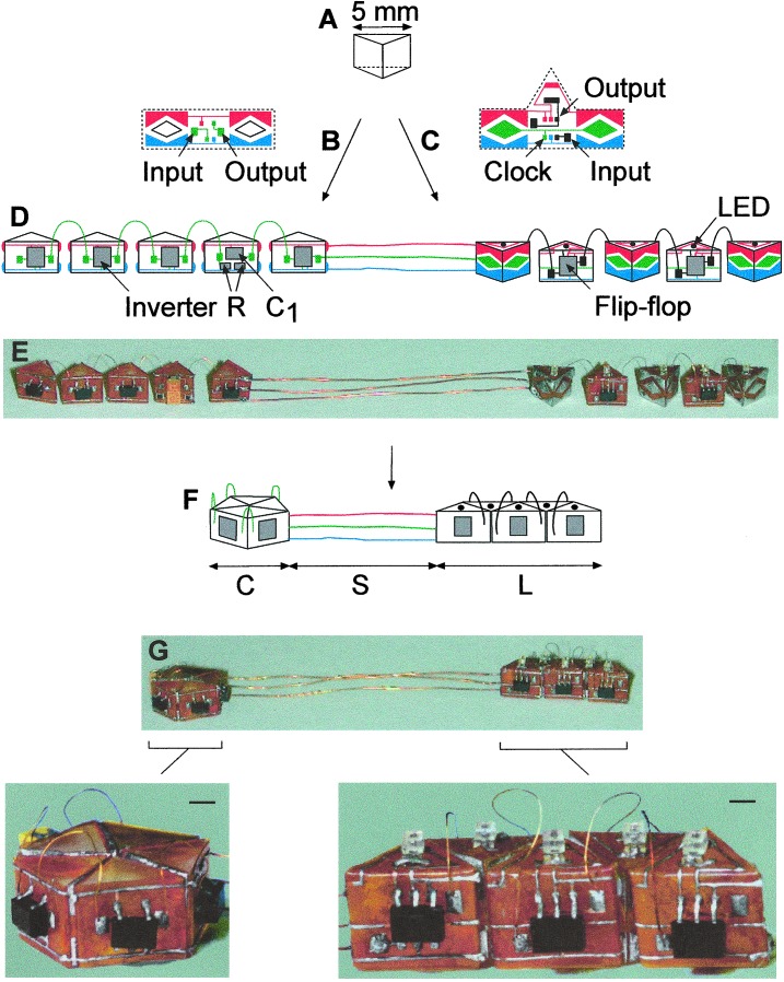
Figure 1.
Design and fabrication of the asymmetrical electronic device. (A) Schematic representation of a triangular prism, the basic unit in the assembly. The prisms were cast in polydimethylsiloxane (PDMS) molds using photocurable polyurethane (J-91, Summers Optical, Fort Washington, PA). (B and C) The solder pattern of contact pads, dots, and wires used for the ring oscillator and the shift register, respectively. A mirror image of the pattern shown in C was used on every second piece in the shift register; this pattern positioned the copper wires connecting input and output of neighboring pieces without crossing above the LEDs, for easier observation. The functions of different parts of the pattern are indicated in color: red, driving voltage; blue, ground; green, clock signal; black, data line. Single inverter gates (SN74AHC1G04, Texas Instruments, Dallas), chip resistors (R1 = 100 kΩ, R2 = 1 MΩ, Skywell, Walnut Creek, CA), a capacitor (C1 = 22 μF, Skywell), D-type flip-flops (NC7SZ175, TinyLogic, Fairchild Semiconductor, South Portland, ME), and LEDs (BL-HS136, American Bright Optoelectronics, Brea, CA), all shown in gray, were soldered onto the patterns contact pads manually. The Clear input of all flip-flops was permanently kept at a High logic level, and only the D-input of the flip-flops was used. The patterns were glued onto the prisms and connected with copper linkers, as depicted in D. Insulated Cu wire (diameter 76 μm, length 10 mm, California Fine Wire, Grover Beach, CA) was used to connect the prisms. Thicker wire (diameter 127 μm, length 40 mm) connected the two flexible pentamers. (E) Photograph of the structure before folding. (F) Schematic drawing of the folded structure, consisting of a circular (C), structural (S), and a linear (L) domain. (G) Photographs of the structure after folding. (Scale bars, 1 mm.)

