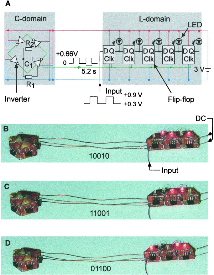
Figure 2.
Operation of the self-assembled electronic device. (A) Circuit diagram of the clocked shift register. The color coding of the electrical connections is as in Fig. 1. The photographs in B–D were taken at intervals of 5.2 s, corresponding to three consecutive clock pulses. The binary numbers stored in the shift register between the clock pulses are visualized by the LEDs, and are indicated on each photograph. Logic level 1 is coded by unlit LEDs, and logic level 0 is given by lit LEDs. The arrows in B indicate the connections made after the self-assembly—to an external voltage source, and to the function generator.

