Abstract
Microporous thin films (≈50 to 400 nm) composed of discrete, cavity-containing molecular rectangles have been prepared. The films, which contain both amorphous and microcrystalline domains, display shape-selective transport behavior. They are permeable to small molecules and to molecules that are short or narrow in at least one dimension—for example, elongated planar molecules—but are impermeable to molecules lacking a narrow dimension. However, the shape selectivity is based on transport through intramolecular rather than intermolecular cavities. By using redox-active probe molecules, rates of transport through the rectangle-based material have been extracted from electrochemical measurements. Spatially resolved measurements obtained via scanning electrochemical microscopy have permitted transport through individual microcrystals to be evaluated semiquantitatively. The measurements reveal that transport is roughly two orders of magnitude slower than observed with thin microcrystalline films of molecular squares featuring similar-sized cavities. The differences likely reflect the fact that cavities within the square-based materials, but not the rectangle-based material, align to form simple one-dimensional channels.
Over the past dozen years a tremendous number and variety of new cyclic, cavity-containing molecules have been intentionally prepared via metal ion coordination chemistry (1–4). Interest in these molecules is partly aesthetic (some remarkable high-symmetry, high-mass, polymetallic compounds have been obtained via extraordinarily efficient directed-assembly and related chemical synthesis techniques), and partly practical [cavity-containing assemblies can function as hosts for smaller molecular or atomic (ionic) guests]. On the practical side, host:guest behavior can be exploited for chemical sensing (5, 6) and for selective chemical catalysis (7), including enzyme-like catalysis (8)—and, indeed, both have been demonstrated for these types of systems in solution-phase environments. When the assemblies are electrically neutral, and therefore lack charge-compensating counter ions that may block cavities, the host behavior can be extended to the solid state. Molecular materials of this kind typically display moderately high void volumes and internal surface areas. Because the coordination bonds defining the component molecules are reasonably strong, cavities are preserved on removal of solvent. This behavior renders the materials functional as hosts for chemical species encountered in the vapor phase, and advantage has been taken of this behavior to construct thin-film sensors for selected volatile organic compounds (9–12).
Because of their nanoscale porosity, the materials are also functional as thin-film molecular sieves—particularly in aqueous solutions where the charge neutrality of the component molecules renders the materials completely insoluble. Sieving behavior has been examined spectrally by using dye molecules together with films supported on macroporous membranes (13). Sieving has also been probed electrochemically by using redox-active molecules together with films supported on electrodes (14, 15); molecules that successfully traverse a film yield a redox response at the underlying electrode (16–18). Consistent with sieving behavior that is primarily defined by the cavities contained within individual host molecules, sharp size cutoffs corresponding to minimum cavity sizes are generally observed. (An exception is sieving by the molecular square compound, [Re(CO)3Cl(μ-pyrazine)]4, which displays a size cutoff that slightly exceeds the molecular cavity size, but is consistent with the minimum dimensions of crystallographically determined interstitial openings.) Investigations to date have been limited to materials composed of tetrametallic molecular squares; the minimum diameters of the corresponding square cavities range from ≈4.5 Å to 23 Å. Notably, single-crystal x-ray structural studies show that square cavities often align in the solid state to create one-dimensional channels (refs. 4, 5, and 16; see Fig. 1). Consistent with channel formation, molecular-square film samples that retain some crystallinity typically transport probe molecules 20 to 50 times faster than amorphous metallopolymeric materials displaying similar molecular size cutoffs (18, 19). Finally, with large squares, cavity functionalization has been demonstrated (20), and the functionalization chemistry has been exploited to tune molecular size cutoffs in a systematic fashion (13, 17, 21).
Figure 1.
Space-filled representations of the molecular and single crystal x-ray structure of the molecular square compound, [Re(CO)3Cl(μ-4,4′-bipyridine)]4, showing the existence of one-dimensional channels. Hydrogens are omitted. Adapted from ref. 16.
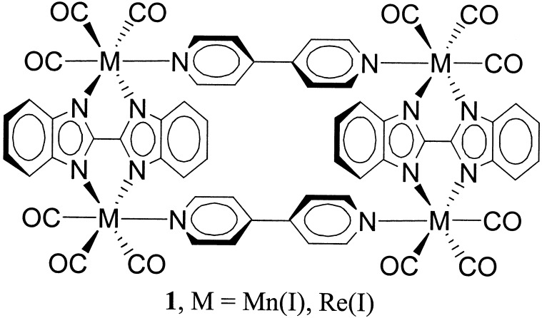
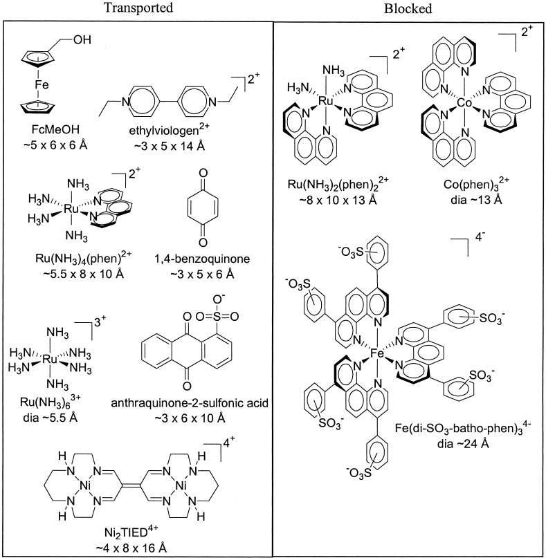
Given the availability of microporous molecular materials showing very good size discrimination properties, it would be both interesting and desirable to develop related materials that additionally show primitive shape discrimination—presumably by employing cavity shapes of lower symmetry than the ubiquitous square geometry. Here, we extend our studies of condensed-phase molecular transport to thin films of molecular rectangles. Synthesis of the rectangles (see structure 1 in Scheme S1) has been described previously, as has their ability to recognize and reversibly sorb selected volatile organic compounds from the vapor phase (11). By using redox-active probe molecules (see Table 1) and conventional voltammetric measurement techniques, we now find that the rectangle-based materials display both size- and shape-selective transport behavior when placed in contact with an aqueous solution environment. Quantitative and semiquantitative measures of molecular transport have been obtained via rotating disk electrode (RDE) voltammetry (22) and via scanning electrochemical microscopy (SECM), respectively (23). The RDE technique yields area-averaged transport rate measurements. The SECM technique, on the other hand, yields spatially resolved transport data, including rates of molecular transport through individual crystalline microstructures.
Scheme 1.
Table 1.
Catalogue of candidate molecular permeants and their dimensions
Those on the left-hand side permeate thin films of the molecular rectangles. Those on the right-hand side are blocked.
Experimental Procedures
Chemicals.
Rectangle 1 was synthesized in both manganese and rhenium form as previously described (11); no difference in transport properties for the two forms was observed. All aqueous solutions were prepared from purified water (18 MΩ, Millipore). [Tris(phen)cobalt(II)](NO3)2⋅6H2O (phen = 1,10-phenanthroline; ref. 24), [tetraammine(phen)ruthenium(II)]Cl2 (25), and [diamminebis(phen)ruthenium(II)]Cl2 (26) were synthesized according to literature methods. Dinickel(II)(1,1′-enebicyclo-3,6,10,13-tetraazatetradeca-2,13-dienylidene) perchlorate was synthesized according to literature methods by workers in the L. O. Spreer group at the University of the Pacific (27). All other materials were obtained from commercial sources. Redox permeant dimensions were estimated by using hyperchem 4 for windows.
Preparation of Electrode-Supported Thin Films.
Thin films of the molecular rectangle were cast from filtered tetrahydrofuran/CHCl3 (1:1 by volume) solutions onto 3-mm diameter glassy carbon rotating disk electrodes. Several drops of solution were placed on the electrode, which was mounted in an inverted electrode rotator (Pine Instrument, Grove City, PA; Model MSRX). The electrode was covered with an opaque test tube and rotated at 50–100 rpm, slowly evaporating the casting solvents. The films were allowed to dry in the dark while rotating for at least 30 min before use. In general, slower evaporation times gave better quality films (i.e., fewer defects). Film thicknesses ranged from 200–400 nm, and were calculated from the surface area of the electrode (and its insulating sheath) and the total amount of material. (The amount of molecular material was determined by dissolving the film in a known volume of tetrahydrofuran, and determination of the concentration was based on UV-visible absorption by using the known molar extinction coefficient.) Film thickness was controlled by application of multiple layers.
Films were also prepared on electrically conductive indium-tin-oxide (ITO)-coated glass slides (Delta Technologies, Stillwater, MN), because the rotating disk electrode geometry was incompatible with SECM and atomic force microscopy (AFM) studies. The slides were cleaned by soaking in a 20/80 (vol/vol) ethanolamine/water solution at 80°C for 15 min, followed by sonication and rinsing with water. Thin films were drop-cast on ITO platforms from tetrahydrofuran/CHCl3 solutions (as above) and allowed to evaporate slowly. After 30 min, the dry films were exposed to tetrahydrofuran vapor for several hours in the dark, causing vapor “annealing” of the films and subsequent crystallite formation, confirmed by low-resolution optical microscopy.
The morphology and microstructure of the thin films prepared on ITO were evaluated via fluorescence microscopy and via tapping mode atomic force microscopy (TMAFM), by using a Digital Instruments (Santa Barbara, CA) Multimode Nanoscope IIIa with single etched silicon (TESP) tips (cantilever length 125 μm and resonance frequency 307 to 367 Hz; Digital Instruments). The thickness of the crystals was determined from cross-section analyses of images, by using digital nanoscope software (version 4.23r2).
Powder Diffraction.
Diffraction patterns from thin films on ITO-coated glass platforms were obtained by using a Rigaku (Tokyo) Geigerflex x-ray diffractometer, using a Cu kα line source and θ/2θ geometry. Scans were obtained over a diffraction angle range of 5–60° by using a step width of 0.2° and an integration time of 4 s.
Electrochemical Measurements.
Electrochemical data were obtained by using a CH Instruments (Austin, TX) Model 900 SECM bipotentiostat with computer data acquisition and control (version 2.04 software). All experiments were performed in aqueous solutions containing 0.2 M KNO3 electrolyte, by using a Pt wire counter electrode and a saturated sodium calomel electrode (SSCE) as a reference. Rotating disk electrode experiments were conducted by using the Pine Instruments analytical rotator.
Scanning electrochemical microscopy tips were prepared from 4-μm radius carbon fibers (Alfa Aesar, Ward Hill, MA) as previously described (19, 28). Smaller tips (with radii ≈0.5 μm) were prepared by cylindrically etching the carbon fiber in 10-mM NaOH solutions according to literature methods (29), and subsequently coated with an insulating polymer as before (19). The tips of the microelectrode tips were freshly exposed before each experiment, and the electroactive radius was determined by using an aqueous solution of ferrocene-methanol according to standard procedure (30). ITO electrodes were mounted in a locally designed cell, filled with the aqueous solution of electrolyte and redox mediator of interest, and the tip was manually lowered to within 100 μm of the surface, using a CCD camera with video output to monitor the approach.
Results and Discussion
Thin Film Materials.
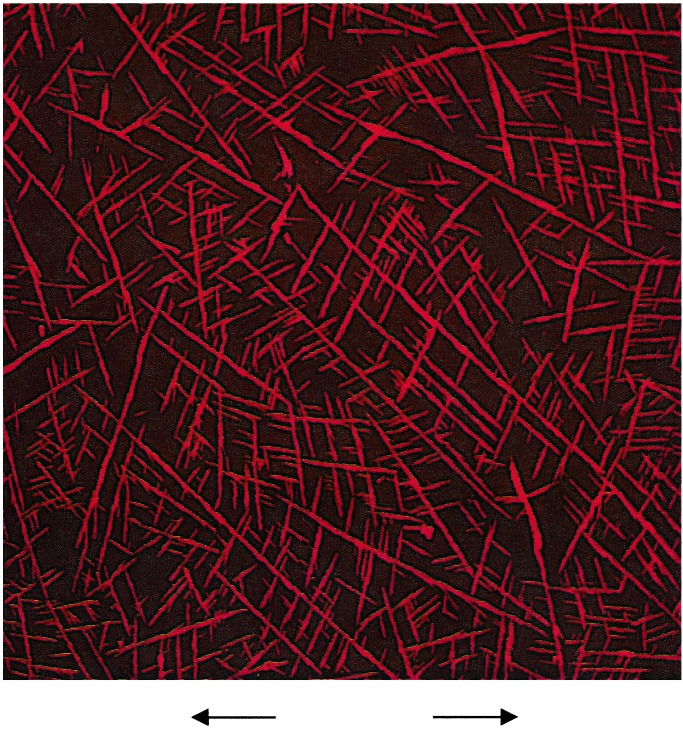
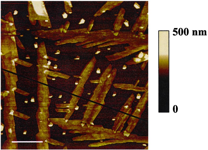
Solvent vapor annealing of drop-cast films of the molecular rectangle on ITO platforms yields a collection of needle-shaped structures that are readily visualized via conventional low-resolution optical microscopy or by luminescence microscopy (see Fig. 2). From the microscopy, the needle widths are a few microns, with lengths of up to 1 mm. A representative expanded image, obtained via atomic force microscopy, is shown in Fig. 3. Consistent with subsequent electrochemical findings, phase-imaging AFM measurements showed that the regions between the needle structures are also composed of rectangles; no exposed ITO was detected. AFM measurements additionally revealed that the needle structures are fairly uniform in height, protruding ≈75 to 100 nm above the surrounding material. X-ray powder diffraction measurements of the microstructured films confirmed their crystallinity, yielding diffraction peaks at the positions expected based on earlier single crystal x-ray diffraction measurements (11). We assume, based on the AFM images, that only the needle structures are crystalline.
Figure 2.
Luminescence microscopy image of a microstructured thin film of the rhenium form of complex 1.
Figure 3.
Tapping mode AFM image of thin film of complex 1.
Voltammetric Transport Screening Studies.
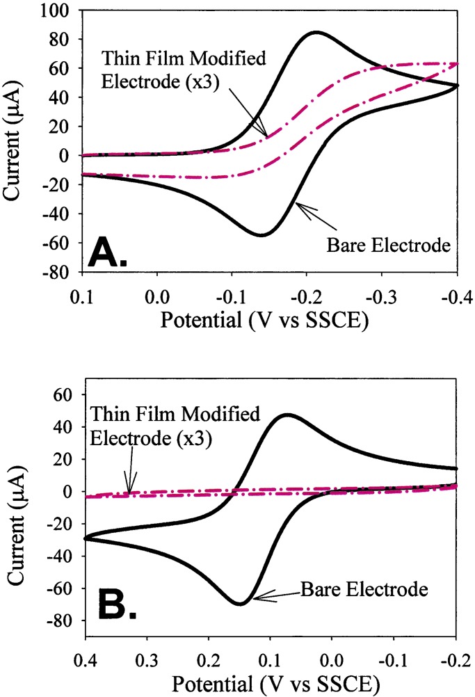
Fig. 4A shows the
cyclic voltammetric responses of naked and film-coated electrodes to a
solution containing Ru(NH3) (approximately spherical; diameter = 5.5 Å). The naked surface
yields peaks in the vicinity of the formal potential for the
Ru(NH3)
 couple. The
coated surface yields an attenuated wave (note change in scale)
featuring a highly distorted, somewhat sigmoidal shape. The observation
of a voltammetric wave indicates that the probe molecule can reach
the underlying electrode surface; the distorted wave shape is
consistent with a transport mechanism that is rate limited by thin-film
permeation (31). Fig. 4B shows the response to a larger
reactant, Co(phen)
 (also approximately spherical;
diameter = 13 Å). Here, the film-coated electrode is completely
blocking with respect to the candidate permeant. The combined results
point to efficient exclusion based on probe molecule size. In addition,
exclusion of the second reactant establishes that, within the detection
limits of the voltammetric experiment, the rectangle-based films are
free from pinhole defects. This point is important, in part, because
pinhole transport represents a possible alternative interpretation for
the observed sigmoidal wave shape in Fig. 4A (32).
Figure 4.
Cyclic voltammograms comparing the response obtained by using a bare
electrode (solid line) and one modified with a thin film of
1 (dashed/dotted line) by using (A) 5 mM
aqueous solution of Ru(NH3) and (B) 5 mM aqueous solution of
Co(phen)
 . Scan rate = 100 mV/s. Electrode
radius = 1.5 mm.
Extension of the studies to an elongated, planar di-nickel probe
molecule and to a similarly elongated and approximately planar viologen
molecule (N,N′-ethyl-4,4′-bipyridinium dication) showed that both can
permeate rectangle-based thin films, despite molecular volumes that
substantially exceed those of
Ru(NH3) . Table 1 shows the
structures of these and several additional probe molecules, lists their
dimensions as determined by molecular modeling, and indicates whether
they permeate rectangle-based coatings. From the summary, it is clear
that thin films of the molecular rectangle selectively transport
candidate permeants both on the basis of permeant size and permeant
shape. Those that are short or narrow in at least one dimension
generally are transported even if they feature larger lengths in other
dimensions.
Whereas it is tempting to ascribe the shape-selective transport
behavior to sieving by the cavities formed by individual molecular
rectangles, a more careful analysis suggests otherwise. The metal sites
within the rectangle define a ligand framework having dimensions of
5.7 × 11.5 Å (11). Inclusion of van der Waals radii for the
atoms comprising the framework substantially decreases the cavity
width, as does a slight inward bowing of the ligands comprising the
long edges of the cavity. The resulting minimum width of ≈1 Å should
exclude even small probe species such as
Ru(NH3) or ferrocene-methanol.
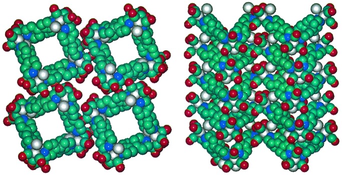
Transport instead appears to be defined primarily by interstitial
cavities (see packing diagram in Fig. 5).
Like the intramolecular cavities, the interstitial cavities feature
elongated, and approximately rectangular, shapes—albeit with larger
widths.
Figure 5.
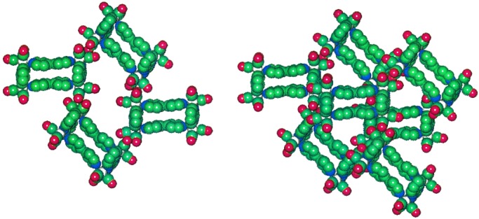
Portions of a packing diagram for 1, derived from single-crystal x-ray data reported in ref. 11. (Left) The packing arrangement for molecules comprising two layers, illustrating that intermolecular cavities exist. (Right) The packing arrangement for molecules comprising three layers, illustrating that simple one-dimensional channels are not formed by the cavities.
Quantitative Transport Studies: Area-Averaged RDE Measurements.
Quantitative information about thin-film molecular transport can be obtained from RDE measurements. Current flow provides a measure of overall molecular flux, i.e., overall molecular transport rate. For sequential transport through solution and permeation of the film, the overall rate (or current, i) can be written as a reciprocal sum of rates or currents (28):
 |
1 |
By creating conditions of controlled convective transport, disk rotation yields well-defined solution-phase fluxes. Furthermore, the flux is tunable—increasing with the square-root of the disk electrode rotation rate, ω. Extrapolation of a plot of itotal−1 vs. ω−1/2 to ω−1/2 = 0 (infinite rotation rate and infinite isoln value) yields ifilm−1.
If the film thickness (d) is known, ifilm can be used to determine the permeability, i.e., the product of the reactant's solution-to-film partition coefficient, P (unitless), and its film-based diffusion coefficient, Df (cm2/s) (31):
 |
2 |
In Eq. 2, n is the number of electrons
transferred per probe molecule (1 for the probes used here),
A is the film-coated electrode area, F is the
Faraday constant, and Cs is the molar
concentration of the probe molecule in solution. (Films used for RDE
measurements were not annealed and therefore lacked the crystalline
microstructures shown in Figs. 2 and 3.) Measurements over a range of
film thicknesses yielded a PDf value
of 4 × 10⁻⁹
cm2⋅s−1 for
Ru(NH3) . Similar experiments
with ferrocene-methanol and Fe(CN)
 yielded values
of 6 × 10⁻⁹ and 2 ×
10−9
cm2⋅s−1,
respectively. These values are roughly three orders of magnitude
smaller than the corresponding values of solution-phase diffusion
coefficients (16). They are roughly two orders of magnitude smaller
than PDf values observed for transport
through films composed of intermediate-sized molecular squares (11, 16,
18–20). As expected, Co(phen)
 yielded no response
in the RDE experiment.
Quantitative Transport Studies: Spatially Resolved SECM Measurements.
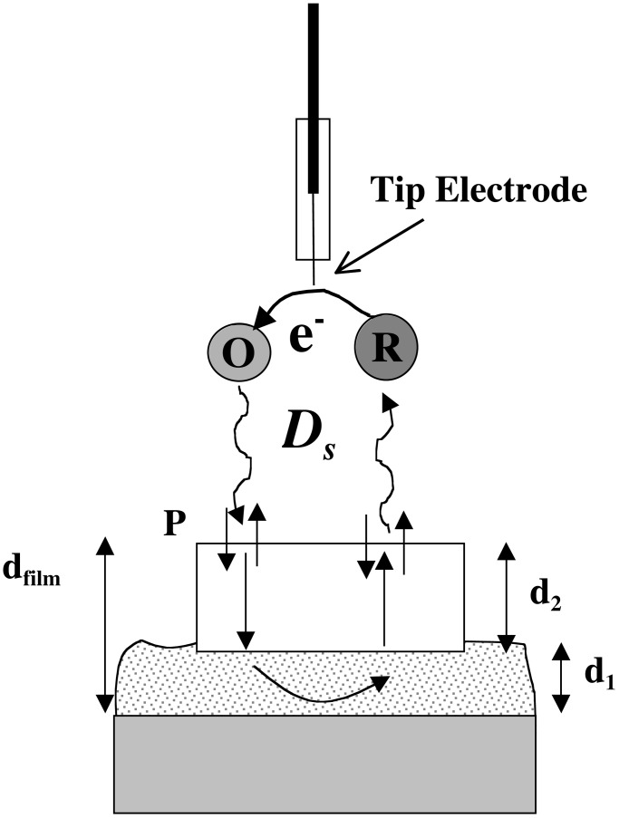
RDE measurements yield area-averaged transport parameters, rather than parameters for a particular section of a potentially heterogeneous film. In contrast, SECM is capable of providing spatially resolved transport information. Briefly, in the form used here, SECM utilizes dual working electrodes (see Fig. 6). One is a tip that can be rastered across a film-coated surface at a separation distance of a few microns (4-μm radius tips) to a few hundred nm (0.5- to 0.6-μm radius tips). The second is the macroscopic electrode supporting the film. Assuming that the solution contains a probe molecule in its reduced form, this electrode is poised at a potential that is sufficiently far positive of the probe's formal potential that any molecule reaching the electrode will be oxidized. The tip electrode, on the other hand, is poised at a potential significantly negative of the formal potential. Consequently, current is observed at the tip electrode only when probe molecules can permeate the film, react, and return to the solution phase in oxidized form.
Figure 6.
Representation of scanning electrochemical microscopy scheme for evaluating molecular transport through individual microcrystallites. O represents redox species initially present in solution; R is the electrochemical reaction product; d2 is the thickness of the crystallite above the amorphous film layer, and is less than or equal to the total film thickness. For simplicity, possible differences in transport parameters for species O vs. R are omitted.
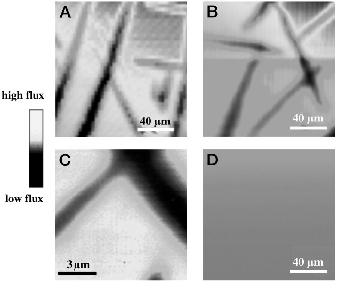
Fig. 7 shows the outcome of a series of
SECM imaging experiments, i.e., plots of tip current vs. tip location.
Fig. 7A and Fig. 7B were recorded with
solutions containing small probe molecules
(Ru(NH3) and
Fe(CN)
 , respectively). These experiments readily
reveal the presence of needle- or ribbon-shaped microcrystalline film
domains. That these domains yield smaller currents or permeant fluxes
is consistent with the expected decrease in flux with increasing film
thickness (Eq. 2). Fig. 7C shows the outcome of a
similar imaging experiment, but recorded at higher resolution. Finally,
Fig. 7D shows the response recorded in the presence of a
large probe molecule, Fe(phen)
 (diameter = 13
Å), expected to be incapable of permeating the rectangle-based film.
In contrast to Fig. 7
A–C, no structure is
evident—only a uniform small background current unrelated to
permeation.
Figure 7.
SECM images of microcrystallites of 1. Images were obtained
by using a 0.6-μm radius carbon fiber tip electrode at a scan rate of
10 μm/s in aqueous solutions of indicated redox probes:
(A) 1.8 mM
Ru(NH3) (Etip = 0 V,
EITO = −0.35 V); (B)5.5 mM
Fe(CN)
 (Etip = 0
V, EITO = +0.4 V); (C)
higher resolution image obtained by using the same solution and applied
voltages as in A, but over smaller scan area and by using a
tip scan rate of 1 μm/s; (D) 4.5 mM
Fe(phen)
 (Etip = 0
V, EITO = 1.0 V). The current response
in D is multiplied times 20.
Semiquantitative Transport Studies: SECM Measurements of Permeability.
As we have noted elsewhere, SECM measurements can also be used to estimate film transport rates (17, 19). The magnitude of the SECM tip current is governed by the rates of sequential film and solution transport processes, and is describable by the reciprocal sum in Eq. 1 (where itotal is now equated with itip). The rate or current associated with solution-phase transport is a complicated function of tip-electrode/generator-electrode (ITO platform) separation distance, reflecting the nature of hemispherical diffusion to the tip, hindering of diffusion by the proximity of the electrodes, and changes in local redox concentration because of feedback (33). Similar to analyses recently published for transport through thin films to an underlying micropatterned generator electrode (19), we found that the ordinarily cumbersome analysis of SECM currents could be greatly simplified via a normalization protocol.
Briefly, to implement the protocol, we first made measurements near a bare platform under “hindered diffusion” conditions, rather than “positive feedback” conditions (i.e., conditions used in the imaging experiments above). In other words, the platform was disconnected electrically, making it impossible for the platform to participate directly in redox processes. At the same time, the tip electrode was poised at a potential where probe molecule oxidation (or reduction, depending on the identity of the molecule) would readily occur. The tip was then translated toward the platform until the tip current was only 85% as large as the current observed at “infinite” distance from the platform. Based on well-established current-distance “approach curves” and associated theory (23, 29–36), the controlled attenuation serves to position the tip electrode at a well-defined and highly reproducible distance above the platform. With the distance fixed, the SECM electrode potentials were switched to positive feedback mode, and the tip current was recorded. From Eq. 1, because the ifilm−1 term is absent for a bare platform, the observed tip current (itotal) can be equated directly with isoln. Notably, the value for isoln at infinite distance for a tip electrode of radius r is: (30)
 |
3 |
Under feedback conditions, with the tip electrode close to the generation electrode, i∞ is enhanced as follows (35, 36):
 |
4 |
 |
5 |
where L is the ratio of tip height above the substrate to tip radius, and k1, k2, k3, and k4 are geometric factors that depend on the relative radii of the tip electrode and its insulating sheath (35, 36). For the quantitative measurements described below, L was generally 1, as in previous work (17).
With this information in hand, the hindered diffusion experiment was repeated with a film-covered electrode, stopping again when the tip current had diminished to 85% of its value at infinite tip-platform separation distance. This protocol serves to position the tip at the same distance from the platform or substrate electrode as in the bare platform experiment. The cell was then switched to feedback mode, and the tip current (itotal in Eq. 1) was again recorded. Given identical separation distances in coated and bare electrode experiments, the values for isoln are likewise identical. The desired value for ifilm can then be obtained from Eq. 1, given the value for itotal at the tip when the generator is a film-covered electrode. By ratioing parameters, approximating ifilm by using Eq. 2, and by using Eqs. 3–5, one can write (19):
 |
6 |
A potentially confusing point is that the area used in Eq. 2 for ifilm is now the area of the tip electrode (19), even though the film covers the macroscopic generator electrode. One could, in principle, focus instead on the generator electrode and calculate the diffusive footprint of the tip electrode on the film-covered generator electrode at a specific separation distance. The footprint area will necessarily exceed the area of the tip electrode, but corrections are needed to account for the fact that not all molecules passing through the footprint region of the film reach the tip electrode. In addition, positive feedback serves to focus the transport toward the center of the footprint. Clearly, in the limit where L approaches zero, the approximation of the effective generator area by the tip area becomes exact. For the approach conditions used here, we have previously found that the approximation works well; the simplified SECM analysis returns transport parameters that agree closely with those obtained from exact analyses of RDE (17, 21) and microelectrode measurements. Given the approximate equivalence under these conditions, we have replaced the difficult footprint/collection-efficiency problem with the simpler problem here of calculating the film flux as if the film were located at the tip electrode.
Eq. 6 is sufficient to approximate transport through an unstructured film of uniform thickness. AFM data show, however, that the microcrystalline needle or ribbon structures extend 75 to 100 nm above the ultrathin (≈50–100 nm) amorphous film layers studied here. If the extra distance is designated d2, and the thickness of the amorphous region is d1, transport through the extended crystalline features is describable by†:
 |
7a |
 |
7b |
Notice that, to apply Eq. 7b, we require knowledge of the crystallite thickness (d2, known from AFM measurements), but not the thickness of the amorphous film (d1). The one assumption made that has not been verified experimentally is that the microcrystallite rests on the amorphous layer, rather than protruding downward through it. If this assumption is not correct, then the transport parameters we attribute solely to the microcrystallites will be contaminated with information about the permeability of the amorphous layer as well.
With this caveat in mind, application of Eq. 7b to SECM data
yielded the following results for molecular transport through
microcrystalline regions of the rectangle-based thin films:
PDf(Ru(NH3) )
≈− 6 × 10⁻⁹
cm2⋅s−1,
PDf(ferrocene-methanol)
≈− 1.1 × 10⁻⁸
cm2⋅s−1,
PDf(Fe(CN)
 )
≈− 2.4 × 10⁻⁹
cm2⋅s−1,
PDf(benzoquinone)
≈− 1.1 × 10⁻⁹
cm2⋅s−1, and
PDf (anthraquinone-sulfonate)
≈− 1.0 × 10⁻⁹
cm2⋅s−1. No film
permeation was detected for Co(phen)
 .
.
The permeabilities measured for transport through crystalline microstructures are only marginally larger than those obtained above, via the RDE method, for area-averaged transport through predominantly amorphous material. Both sets of parameters are much smaller than found for transport through thin films of similar sized molecular squares (16). Both observations likely reflect the absence of channels in the microcrystalline rectangle-based material. Under these conditions, crystallinity confers little advantage: permeants experience tortuous transport paths regardless of whether crystalline order exists. The absence of channels also likely accounts for the much slower rates for transport through thin films of the molecular rectangle vs. thin films of similar-sized molecular squares.
Conclusions
Thin films of cavity-containing molecular rectangles display shape-selective transport behavior. The films are permeable to small molecules and to molecules that are short or narrow in at least one dimension—for example, elongated planar molecules. They are impermeable to molecules lacking a narrow dimension. The shape selectivity, however, is based on transport through intramolecular rather than intermolecular cavities. By using redox-active probe molecules, rates of transport through the rectangle-based material can be extracted from electrochemical measurements. Spatially resolved measurements obtained via scanning electrochemical microscopy permit parameters for transport through individual microcrystals to be estimated. The measurements reveal that transport is roughly two orders of magnitude slower than observed with thin microcrystalline films of molecular squares featuring similar-sized cavities. The differences likely reflect the fact that cavities within the square-based materials, but not the rectangle-based material, align to form simple one-dimensional channels.
Acknowledgments
We gratefully acknowledge Dr. Xiaojun Dang for collecting x-ray powder diffraction data, and Aaron Massari and Dr. Keith J. Stevenson for collecting AFM and fluorescence microscopy images. We thank Prof. Larry Spreer at the University of the Pacific for providing samples of [Ni2TIED](ClO4)4. We thank an anonymous reviewer for helpful comments. We thank the National Science Foundation and Northwestern University for financial support of our work.
Abbreviations
- RDE
rotating disk electrode
- ITO
indium tin oxide
- AFM
atomic force microscopy
- SECM
scanning electrochemical microscopy
Footnotes
This paper was submitted directly (Track II) to the PNAS office.
In formulating Eq. 7, we intentionally neglected the effect of small differences in film thickness on the tip-platform separation distance and, therefore, isoln. That the difference can be safely neglected is confirmed by imaging experiments run in “hindered diffusion” mode (where itotal = isoln). In contrast to experiments run in “positive feedback” mode (see Fig. 7), the hindered diffusion mode images are featureless, indicating that the surface height differences are too small to alter isoln to a detectable degree.
References
- 1.Leininger S, Olenyuk B, Stang P J. Chem Rev. 2000;100:853–907. doi: 10.1021/cr9601324. [DOI] [PubMed] [Google Scholar]
- 2.Fujita M. Chem Soc Rev. 1998;27:417–425. [Google Scholar]
- 3.Holliday B J, Mirkin C A. Angew Chem Int Ed Engl. 2001;40:2022–2043. [PubMed] [Google Scholar]
- 4.Dinolfo P H, Hupp J T. Chem Mater. 2001;13:3113–3125. [Google Scholar]
- 5.Slone R V, Yoon D I, Calhoun R M, Hupp J T. J Am Chem Soc. 1995;117:11813–11814. [Google Scholar]
- 6.Chang S H, Chung K-B, Slone R V, Hupp J T. Synth Met. 2001;117:215–217. [Google Scholar]
- 7. Ito, H., Kusukawa, T. & Fujita, M. (2000) Chem. Lett. 598–599.
- 8.Merlau M L, Mejia M d P, Nguyen S T, Hupp J T. Angew Chem Int Ed Engl. 2001;40:4239–4242. doi: 10.1002/1521-3773(20011119)40:22<4239::AID-ANIE4239>3.0.CO;2-E. [DOI] [PubMed] [Google Scholar]
- 9.Sun S-S, Lees A J. J Am Chem Soc. 2000;122:8956–8967. [Google Scholar]
- 10.Keefe M H, Slone R V, Hupp J T, Czaplewski K F, Snurr R Q, Stern C L. Langmuir. 2000;16:3964–3970. [Google Scholar]
- 11.Benkstein K D, Hupp J T, Stern C L. Angew Chem Int Ed Engl. 2000;39:2891–2893. doi: 10.1002/1521-3773(20000818)39:16<2891::aid-anie2891>3.0.co;2-q. [DOI] [PubMed] [Google Scholar]
- 12.Mines G A, Tzeng B-C, Stevenson K J, Li J, Hupp J T. Angew Chem Int Ed Engl. 2002;41:154–157. doi: 10.1002/1521-3773(20020104)41:1<154::aid-anie154>3.0.co;2-f. [DOI] [PubMed] [Google Scholar]
- 13.Czaplewski K F, Snurr R Q, Hupp J T. Adv Mater. 2001;13:1895–1897. [Google Scholar]
- 14.Pressprich K A, Maybury S G, Thomas R E, Linton R W, Irene E A, Murray R W. J Phys Chem. 1989;93:5568–5574. [Google Scholar]
- 15.Gould S, Meyer T J. J Am Chem Soc. 1991;113:7442–7443. [Google Scholar]
- 16.Bélanger S, Hupp J T, Stern C L, Slone R V, Watson D F, Carrell T G. J Am Chem Soc. 1999;121:557–563. [Google Scholar]
- 17.Williams M E, Hupp J T. J Phys Chem B. 2001;105:8944–8950. [Google Scholar]
- 18.Bélanger S, Anderson B C, Hupp J T. In: Molecular Functions of Electroactive Thin Films. Oyama N, Birss V I, editors. Vol. 98. Boston: Electrochem. Soc.; 1999. –26, pp. 208–214. [Google Scholar]
- 19.Williams M E, Stevenson K J, Massari A M, Hupp J T. Anal Chem. 2000;72:3122–3128. doi: 10.1021/ac9914622. [DOI] [PubMed] [Google Scholar]
- 20.Bélanger S, Keefe M H, Welch J L, Hupp J T. Coord Chem Rev. 1999;190–192:29–45. [Google Scholar]
- 21.Bélanger S, Hupp J T. Angew Chem Int Ed Engl. 1999;38:2222–2224. [PubMed] [Google Scholar]
- 22.Bard A J, Faulkner L R. Electrochemical Methods, Fundamentals and Applications. 2nd Ed. New York: Wiley; 2001. pp. 331–354. [Google Scholar]
- 23.Bard A J, Denuault G, Lee C, Mandler D, Wipf D O. Acc Chem Res. 1990;23:357–363. [Google Scholar]
- 24.Wheeler S H, Zingheim S C, Nathan L C. J Inorg Nucl Chem. 1978;40:779–783. [Google Scholar]
- 25.Doorn S K, Hupp J T. J Am Chem Soc. 1989;111:4704–4712. [Google Scholar]
- 26.Dwyer F P, Goodwin H A, Gyarfas E C. Aust J Chem. 1963;16:544–548. [Google Scholar]
- 27.McAuley A, Xu C. Inorg Chem. 1992;31:5549–5554. [Google Scholar]
- 28.Potje-Kamloth K, Janata J, Josowicz M. Ber Bunsenges Phys Chem. 1989;93:1480–1485. [Google Scholar]
- 29.Schulte A, Chow R H. Anal Chem. 1998;70:985–990. doi: 10.1021/ac970934e. [DOI] [PubMed] [Google Scholar]
- 30.Wightman R M, Wipf D O. In: Electroanalytical Chemistry. Bard A J, editor. Vol. 15. New York: Dekker; 1980. pp. 267–353. [Google Scholar]
- 31.Gough D A, Leypoldt J K. Anal Chem. 1979;51:439–444. [Google Scholar]
- 32.Saveant J M. J Electroanal Chem Interfacial Electrochem. 1991;302:91–101. doi: 10.1016/0302-4598(87)85005-5. [DOI] [PMC free article] [PubMed] [Google Scholar]
- 33.Bard A J, Fan F-R F, Mirkin M V. In: Electroanalytical Chemistry. Bard A J, editor. Vol. 18. New York: Dekker; 1994. pp. 243–264. [Google Scholar]
- 34.Barker A L, Gonsalves M, Macpherson J V, Slevin C J, Unwin P R. Anal Chim Acta. 1999;385:223–240. [Google Scholar]
- 35.Amphlett J L, Denuault G. J Phys Chem B. 1998;102:9946–9951. [Google Scholar]
- 36.Martin R D, Unwin P R. Anal Chem. 1998;70:276–284. [Google Scholar]


