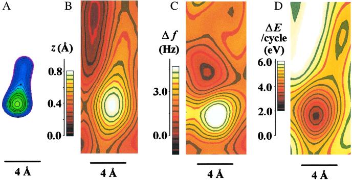
Fig 5.
(A) Simulation of a topographic image of a single adatom on silicon recorded with a laterally oscillating tip (amplitude, 3 Å; tilt angle, θ = 6°). Both the tip and sample states were assumed to have a p-type symmetry, yielding a tunneling matrix element proportional to cos4(ϕ)e−2κr (20), where ϕ is the angle between the vector connecting tip and sample atom and the surface normal, r is the distance between tip and sample atom, and κ is the decay constant of the tunneling current (here, κ = 1 Å−1 is used as a typical value after ref. 20). The image is a map of constant average tunneling current. The position of the adatom is depicted with a black dot. The distance of the adatom and the maximum height in the image is 2.4 Å, i.e., 20% less than the oscillation amplitude A. The vertical distance between the contour lines is equal to that shown in B (5 pm). Thermal excitation and quantum mechanical zero-point motion are not considered in this simulation; therefore the simulated image is sharper than the experimental image shown in B. (B) Experimental topographic image of a silicon adatom with θ ≈ 6° and A ≈ 3 Å (enlargement of the adatom marked with a blue arrow in Fig. 3A). The oscillation of the cantilever is not exactly parallel to the y (vertical) axis but is rotated by −10°. (C) Frequency-shift image of a single adatom on silicon recorded with a laterally oscillating tip (amplitude, 3 Å; tilt angle, θ ≈ 6°) showing exactly the same area as in B. The location where maximum positive frequency shift occurs does not coincide exactly with the maximum in the topography. (D) Corresponding damping data, again showing exactly the same section as B and C. Minimum damping occurs at the site where the frequency shift is maximal.

