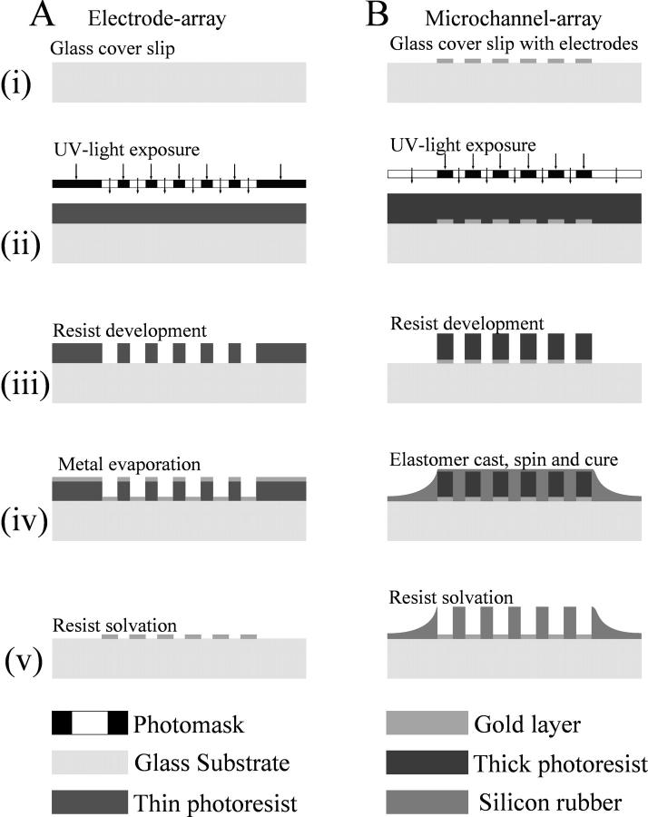
FIGURE 1.
Schematic diagram outlining the fabrication processes of the array of the electrodes (A) and the array of the microchannels (B). The height of the channels was defined by the thickness of the patterned photoresist film used as a master for replica molding of PDMS (B, iii). PDMS was cast against the master and the cured polymer was thoroughly washed in acetone to remove all residual resist and to clear the surface of the microelectrodes (B, v). Without the support of the photoresist, the thin film of PDMS covering the microchannels collapsed and was easily washed off. The PDMS film covering the bulk electrodes served as an insulating layer to avoid short circuits of the leads through buffer spill.

