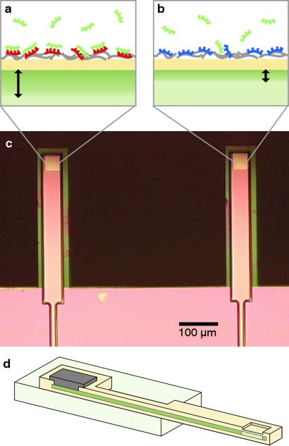
Fig 1.
Sensor schematics. (a and b) EIS interface of a n-type field-effect sensor. DNA exhibits one intrinsic negative charge per base at its sugar-phosphate backbone. Probe DNA is bound electrostatically to a layer of PLL (gray) on the surface. (a) Binding of negatively charged target DNA (green) to its complementary probe DNA (red) at the sensor surface (yellow) extends the depletion region (black arrow) in the silicon portion of the sensor compared with b, where no binding occurs to noncomplementary probe DNA (blue). (c) Optical micrograph of a device consisting of field-effect sensors at the terminus of two cantilevers. The cantilevers are 500 μm long, 75 μm wide, and 3 μm thick. (d) Cross section of a cantilever field-effect sensor. The sensing area at the terminus of the cantilever is connected electrically to a metal contact on the substrate by a layer of highly doped silicon inside the cantilever.

