Abstract
Directed assembly of nanoscale building blocks such as single-walled carbon nanotubes (SWNTs) into desired architectures is a major hurdle for a broad range of basic research and technological applications (e.g., electronic devices and sensors). Here we demonstrate a parallel assembly process that allows one to simultaneously position, shape, and link SWNTs with sub-100-nm resolution. Our method is based on the observation that SWNTs are strongly attracted to COOH-terminated self-assembled monolayers (COOH-SAMs) and that SWNTs with lengths greater than the dimensions of a COOH-SAM feature will align along the boundary between the COOH-SAM feature and a passivating CH3-terminated SAM. By using nanopatterned affinity templates of 16-mercaptohexadecanonic acid, passivated with 1-octadecanethiol, we have formed SWNT dot, ring, arc, letter, and even more sophisticated structured thin films and continuous ropes. Experiment and theory (Monte Carlo simulations) suggest that the COOH-SAMs localize the solvent carrying the nanotubes on the SAM features, and that van der Waals interactions between the tubes and the COOH-rich feature drive the assembly process. A mathematical relationship describing the geometrically weighted interactions between SWNTs and the two different SAMs required to overcome solvent–SWNT interactions and effect assembly is provided.
Keywords: self-assembly, rings, structured thin films, Monte Carlo simulations
Single-walled carbon nanotubes (SWNTs) show promise for applications ranging from ultra-small electronic and sensing devices to multifunctional materials (1). To date, a number of SWNT-based proof-of-concept devices (2–7) such as field effect transistors (2), field emission displays (7), and chemical sensors (3, 6) have been fabricated, and the integration of the nanotube materials in all cases relies on one’s ability to control the placement, orientation, and shape of the nanotube components within the context of the device on the micrometer- to nanometer-length scale. Such positional control over large areas is extremely challenging and currently quite limited. Depending on the intended application, one wants to be able to pattern SWNTs as individual tubes (3, 4), small bundles (5), or thin films (6, 8, 9). Previous studies have shown that individual carbon nanotubes can be positioned (10), bent (11), and even welded (12) with nanometer accuracy by using scanning probe instruments. This level of manipulation is limited to serial and therefore slow processes that span relatively short distances (100 μm). Other assembly methods such as Langmuir–Blodgett techniques (13), external field assisted routes (14–19), electrospinning (20), transfer printing (21), and DNA templates (22, 23) also have been explored for nanotube assembly. These parallel methods address the speed limitation posed by conventional scanning probe techniques, but thus far are quite limited with respect to registration control and have demonstrated only coarse placement capabilities. One promising approach to overcoming these limitations is to use patterned chemical templates to assemble SWNTs from solutions. For example, SWNTs have been successfully positioned along straight line features comprised of amine-terminated self-assembled monolayers (SAMs) (9, 24–27). Thus far, however, no one has demonstrated the ability to simultaneously control the position, shape, and linkage of SWNTs on the sub-μm scale. Such capabilities would allow one to construct much more sophisticated architectures from SWNTs, including rings, electronic interconnects, and structured thin films. The method presented here is based on an interesting observation that SWNTs are attracted to the hydrophilic portions of a gold substrate patterned by dip pen nanolithography (DPN) (28, 29) and more specifically to the boundary between hydrophilic and hydrophobic SAM features made of 16-mercaptohexadecanoic acid (MHA) and 1-octadecanethiol (ODT), respectively. Importantly, the process uses solvent as a preferred carrying media for the carboxylic acid-terminated features and allows one to control the manipulation and assembly (aligning, positioning, shaping, and linking) of SWNTs on the μm- to sub-100-nm length scale, and in some cases, over large areas by using microcontact printing (μCP) (30) and parallel DPN (31).
Results and Discussion
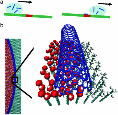
To evaluate the prospect of using SAM boundaries for controlling the assembly of SWNTs, we used DPN to generate patterns of MHA consisting of lines, dots, rings, and even alphabetical letters on a gold substrate. The exposed gold regions of the substrate were passivated with ODT. A drop of 1,2-dichlorobenzene containing SWNTs was then rolled over the patterned substrates (Fig. 1a). Because 1,2-dichlorobenzene wets the MHA features but not the ODT passivated regions, SWNTs are guided and localized on the hydrophilic regions of the substrate. As the solution containing the SWNTs evaporates, the nanotubes are attracted both to each other and the boundary between the ODT and MHA. This evaporation creates a high local concentration of the SWNTs at the SAM boundaries and almost exclusive assembly on the MHA features (Fig. 1b). There is a strong van der Waals attraction between the SWNTs and the carboxylic acid moieties of the MHA, which is apparent in molecular modeling studies (see below). Because the tubes are too long to assemble within an individual feature they are organized at the interface of the SAMs and bent along the perimeter of the features to maximize the overlap with the MHA feature and minimize the tension arising from nanotube bending. In the case of dots or rings, this assembly process results in circular structures and substantial bending of the SWNTs, the extent of which depends on the radius of curvature (Figs. 2 and 3). Note that within these features the SWNTs follow the perimeter of the dot and form continuous architectures through intertube linking.
Fig. 1.
Schematic diagram of the directed assembly process. (a) Schematic illustrating the rolling of a drop of the SWNTs∕1,2-dichlorobenzene solution on a two-component surface, COOH-SAM (red) and CH3-SAM (green). (b) The SWNTs (blue) are selectively transported to the COOH-SAM and pinned at its boundary with the ODT SAM. Upon drying, the SWNT bends to precisely follow the molecular path of the patterned COOH-SAM.
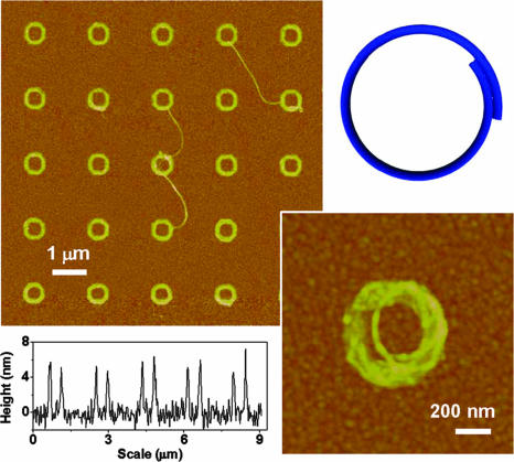
Fig. 2.
SWNTs assembled into rings and nano letters. (Left) AFM tapping mode topographic images (Upper) and height profiles (Lower) of SWNT rings in a 5 × 5 array are shown. (Right) A zoom-in view of one SWNT ring (Lower) and a molecular model of a coiled SWNT (Upper).
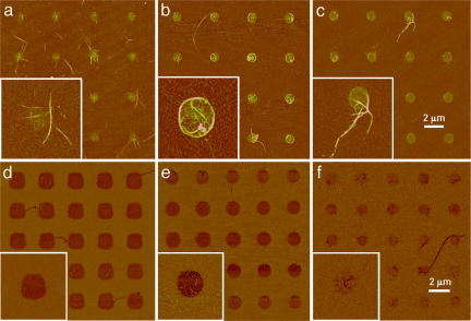
Fig. 3.
The assembly of SWNTs depends critically on the surface functional groups. (a–c) AFM tapping mode topographic images of a series of substrates with 1-μm MHA dot arrays passivated with MUO (a), ODT (b), and PEG-SH (c). These dots show that ODT is the superior passivation layer. (d–f) AFM phase images of a second series of 2-μm dots of MUO (d), AUT (e), and PEG-SH (f), passivated with ODT. None of these show the optimized SWNT assembly observed for the MHA∕ODT system in b. (Insets) Shown are zoom-in images of a selected dot. All images were taken at a scan rate of 0.5 Hz. The height scale is 20 nm, and the phase lag is 10°.
Circular structures made of SWNTs are unusual (17, 18, 32). These structures show interesting curvature-dependent magnetic and electronic properties (33, 34). Rings of SWNTs, ≈500 nm in diameter, were first observed as a low-yield side product in nanotube synthesis (32). Recently, ring structures were produced in solution by an ultrasonication method (17) and ring closure reactions (18). With our approach, such SWNT rings can easily be formed and positioned in an ordered array on a surface (Fig. 2a). For example, 1- to 3-μm-long nanotubes form ring structures on 170-nm-wide, 650-nm-diameter MHA ring features on an Au surface, with exposed Au passivated with ODT. The average height of each SWNT ring is 6 ± 2 nm, demonstrating that these are stacked intertwined structures. They are about five times thinner than the analogous structures formed by ultrasonication (17). By using shorter SWNTs (≈0.4–1.5 μm), we have further demonstrated that SWNTs readily bend to form sub-μm-sized arcs. Even greater control is demonstrated by shaping SWNTs into nano letters with this approach (see Figs. 6 and 7, which are published as supporting information on the PNAS web site).
To fully understand and use this system, we need to elucidate the driving force for the assembly process and the resolution at which SWNTs can be patterned. To address the resolution issue, we used DPN to pattern Au substrates with MHA dots and lines with different dimensions over the micrometer to sub-100-nm length scale. This technique allows one to study the process in combinatorial format under one set of experimental conditions. These experiments clearly show that SWNTs assemble on all features studied, including the smallest dots (90 nm in diameter) and the thinnest lines (450 × 100 nm) (see Figs. 8 and 9, which are published as supporting information on the PNAS web site).
We found that the choice of affinity template SAM and passivating SAM pair is critical for achieving this level of precision in the manipulation and assembly of SWNTs. When the passivation layer was 1-mercaptoundecanol (MUO) or 11-mercaptoundecyl-penta-ethyleneglycol (PEG-SH), the SWNTs assembled on the MHA features but not along the edges of such structures as in the case of the ODT∕MHA system (Fig. 3 a–c). Although dots of MUO, PEG-SH, and 11-amino-1-undecanethiol (AUT), where the gold substrate was passivated with ODT, all show affinities for the SWNTs, the interaction seems weaker as compared with MHA as evidenced by a lower density of SWNTs on such features (Fig. 3 d–f). Surprisingly, although NH2-SAMs were the focus of previous studies (24–26), MHA shows a higher tendency than AUT to assemble and surface-confine SWNTs.
Contact angle measurements show that 1,2-dichlorobenzene wets all but the ODT SAMs on gold. The static contact angle for 1,2-dichlorobenzene on ODT SAMs was determined to be 60 ± 2°, whereas the contact angles for the other SAMs were all <10°. Because the solvent wets the COOH-SAMs but not the CH3-SAMs, no solvent remains on the CH3-SAM as the substrate is pulled from the SWNT solution. In contrast, all of the other surfaces retain a thin liquid film, which results in nonuniform SWNT assembly. Compared with the SAMs of MUO, PEG-SH, and AUT, dot features of such materials with surrounding regions passivated with ODT show higher densities of SWNTs on the affinity template portions of the surface (see Fig. 10, which is published as supporting information on the PNAS web site). These observations strongly suggest that the solvent∕substrate interactions are in part responsible for localizing the SWNTs on the MHA patterns.
When a SWNT is driven close to the MHA pattern in the ODT∕MHA system, Monte Carlo simulations show that van der Waals attractions between the MHA and SWNT provide the driving force for assembly. Using a parallel Monte Carlo program package and the Amber force field (35), we obtained the following relative interaction energies between a [9,6] SWNT and its surroundings: −0.88 eV per nm SWNT for ESWNT/solvent (the interaction of a SWNT with the 1,2-dichlorobenzene solvent), −0.84 eV per nm SWNT for ESWNT/CH3-SAM (the interaction with a CH3-SAM), and −1.05 eV per nm SWNT for ESWNT/COOH-SAM (the interaction with a COOH-SAM). This ordering, COOH-SAM ≫ solvent > CH3-SAM, favors SWNT adsorption from solvent onto the COOH-SAM and not the CH3-SAM. Interestingly, the interaction of a SWNT with AUT, −0.87 eV per nm SWNT, is much weaker than that for MHA, manifesting the important role of van der Waals interactions in the assembly of SWNTs. In addition, if the tube is sufficiently long (length greater than the size of the MHA feature) and flexible, it will maximize its interaction with the COOH-SAM and minimize strain energy by aligning with the outer boundary of the COOH-SAM.
By balancing these interaction energies, it is possible to predict the size of a COOH-SAM required for trapping a SWNT of a given length. For a SWNT with a fraction χ of its length in van der Waals contact with the COOH-SAMs and the remainder, 1 − χ, in contact with the CH3-SAMs, the thermodynamic requirement for assembly is,
 |
Solving Eq. 1 gives χ ≥ 19%. This χ value indicates that a [9,6] SWNT can be stabilized on the surface even if only 19% of its length is in contact with the COOH-SAMs. In other words, a 19-nm-wide stripe of the COOH-SAM is sufficient for trapping a [9,6] SWNT that is 100 nm in length, even in the extreme situation where the nanotube is perpendicular to the stripe. For a SWNT making a smaller angle with respect to the stripe, trapping requires an even smaller stripe width.
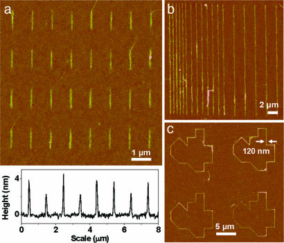
Based on the aforementioned observations, this approach appears ideal for the assembly of SWNTs in a dense array on surfaces. Indeed, Fig. 4a shows an array of parallel aligned SWNTs assembled on MHA patterns (1 μm × 130-nm lines at a line density of 5.0 × 10⁷∕cm2) with nearly 100% occupancy. Atomic force microscopy (AFM) heights are consistent with individual SWNTs or small bundles on each feature. We found that the line width of MHA required for the assembly is only ≈1∕10 that of the NH2-SAMs, resulting in a density >10 times higher than what could be achieved previously (25). The decrease in required line width is essential for the precise assembly of short SWNTs (10–50 nm) for high-performance field effect transistors (36).
Fig. 4.
AFM tapping mode topographic images of selected SWNT arrays. (a) Parallel aligned SWNTs with a line density approaching 5.0 × 10⁷∕cm2. (b) Linked SWNTs following MHA lines (20 μm × 200 nm) spaced by 2 μm, 1 μm, and 600 nm. (c) Random line structure, showing the precise positioning, bending, and linking of SWNTs to a MHA affinity template. All images were taken at a scan rate of 0.5 Hz. The height scale is 20 nm.
As the size of the MHA pattern is increased, the same spot is often occupied by additional SWNTs, with the number being approximately proportional to the volume of the trapped solution. Because of the strong van der Waals attraction between SWNTs (−1.22 eV per nm contact), additional SWNTs can be deposited on the same site, intertwining with each other, and extending to bridge SWNTs on nearby MHA features. As a result, the spacing between SWNTs cannot be reduced to a distance much smaller than the tube length without effecting feature cross-linking or sacrificing SWNT feature occupancy. To reduce the van der Waals attraction, we functionalized the SWNT sidewalls with dodecyl groups as described (37). The functionalization increased the solubility of SWNTs in 1,2-dichlorobenzene and resulted in more uniform assembly. Because the dodecyl groups can be thermally cleaved from the tubes at 200°C (37), these groups act as nondestructive spacers for fine-tuning the interactions between the tubes. Alternatively, one can take advantage of van der Waals attraction to link tubes to make more sophisticated interlinked structures. For example, μm-long SWNTs were assembled into arrays of continuous, parallel aligned, sub-μm-spaced nanowires (Fig. 4b and see Fig. 11, which is published as supporting information on the PNAS web site). Because of the unusual electrical properties of SWNTs, including an electrical conductivity rivaling copper and a current carrying capacity up to 109 A∕cm2 for metallic SWNTs (38), this technique may enable SWNTs to be used as conductive interconnects in electronics. In another example, individual and bundled SWNTs were linked to follow an MHA path defined by DPN, exhibiting extensive flexibility that is favorable for making electronic interconnects (Fig. 4c and also see Fig. 12, which is published as supporting information on the PNAS web site).
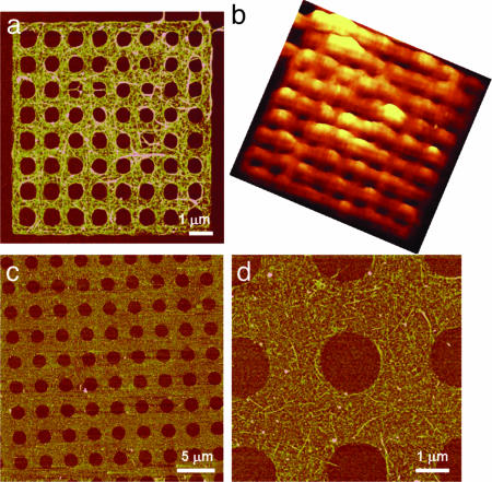
The ability to control the shape of SWNTs allows one to engineer their band gaps by building in strain (39) but, most importantly, this assembly method provides researchers with a tool to organize SWNTs into desirable architectures for a variety of potential applications. For example, this approach provides a simple route toward creating thin structured SWNT films that are currently unattainable. Fig. 5a demonstrates a “proof-of-concept” SWNT filtration membrane with a thickness of only 9 ± 2 nm. The SWNT composition has been characterized and mapped with a Raman confocal microscope (Fig. 5b). These membranes can be made uniformly over 1 × 2 cm by μCP (Fig. 5 c and d), and their sizes appear to be limited only by the area and patterned structures defined by available lithography techniques. The thickness of these membranes can be controlled down to ≈5–10 nm, thereby promising an ultra-high flux in filtration (40) and structured, transparent conductors potentially useful in flexible displays (8, 41).
Fig. 5.
Proof-of-concept SWNT filtration membranes. (a) AFM topographic image of a SWNT membrane with 600 ± 50-nm-diameter pores spanning an area of 10 × 10 μm. (b) Corresponding Raman image showing SWNT spectroscopic signatures. The false color topography represents the integrated Raman intensity over 1,320–1,620 cm−1. (c and d) Representative AFM topographic images of a SWNT network with 1.6 ± 0.1-μm-diameter pores spanning an area of 1 × 2 cm. All AFM images were recorded at a scan rate of 0.5 Hz, and the height scales are 20 nm.
In conclusion, we have demonstrated the ability to position, shape, and link μm-long SWNTs by using the boundaries between COOH- and CH3-SAMs as affinity templates. Experiments and molecular simulations show excellent control down to sub-100-nm dimensions. Further control may be possible by fine-tuning the intertube interactions (42) and coupling to other alignment techniques such as Langmuir-Blodgett methods (13) or microfluidics (43). Because there is no specific chemical bonding required, this technique may prove effective for the directed assembly of other nanoscale building blocks such as nanowires and nanoparticles.
Materials and Methods
Materials.
MHA (90%), ODT (98%), MUO (97%), 1,2-dichlorobenzene (99%), and ethanol (200 proof, HPLC grade) were purchased from Sigma-Aldrich. AUT (99%) was purchased from Dojindo Laboratories, Kumamoto, Japan. Ti (99.7%) and Au (99.99%) wires were purchased from Alfa Aesar, Ward Hill, MA. PEG-SH was prepared as described (44).
SWNT Functionalization and Solution Preparation.
Purified HiPco materials (45), with an iron impurity <1.4 wt%, were dispersed in 1,2-dichlorobenzene by mild sonication using a bath sonicator (Branson model 2510) for 3 min. The resulting dispersion was then centrifuged at 50,000 × g for 10 min, and the supernatant was sonicated for 3 min. This process was repeated twice, resulting in a solution containing a high percentage of individual∕small bundles of SWNTs. To minimize SWNT aggregation in solution, low concentrations (5–20 mg∕liter) were used. Further improvement in solution uniformity was achieved by sidewall functionalization of SWNTs with dodecyl groups (37).
DPN.
DPN (28, 29) experiments were performed with an atomic force microscope (CP-III, Veeco∕Thermomicroscopes, Sunnyvale, CA) equipped with a 100-μm scanner and closed-loop scan control and commercial lithography software (dpnwrite, DPN System-1, NanoInk, Chicago). Gold-coated commercial AFM cantilevers (sharpened, Si3N4, type A, NanoInk) with a spring constant of 0.05 N∕m were used for patterning and subsequent imaging. All DPN patterning experiments were carried out under ambient conditions (≈30% relative humidity, 20–24°C). Tips were soaked in an ink solution (e.g., saturated solution of MHA in acetonitrile) for 20 s, and then blown dry with N2. MHA features were generated on a gold thin film by traversing the tip over the surface in the form of the desired pattern. Polycrystalline Au films were prepared by thermal evaporation of 10 nm of Ti on SiOx followed by 30 nm of Au at a rate of 1 Å∕s and a base pressure ≤ 1 × 10⁻⁶ Torr.
μCP.
Stamps were fabricated in a similar process as described (30). The stamp was “inked” with 5 mM total alkanethiol solution by gently spreading a drop on the surface of the stamp with a Q-tip. After the stamp was dry, patterned structures were generated on the surface by bringing the stamp (by hand) into contact with a clean Au thin film for 10 s. Then, the substrate was rinsed with ethanol and dried with N2. The regions surrounding the molecular features patterned by DPN or μCP were passivated with a monolayer of alkanethiol molecules (e.g., ODT) by immersing the substrate in a 1-mM ethanol solution for 10 min followed by copious rinsing with ethanol and water (Barnstead Nanopure Water Purification System), alternatively. Finally, the substrate was dried with N2.
Monolayer Formation.
SAMs of alkanethiol molecules were prepared on Au thin films by immersing the substrate in a 1-mM ethanol solution of the corresponding molecules for 1 h, followed by rinsing with ethanol and drying with N2. Static contact angles were measured by using the half-angle technique (Tantec, Schaumberg, IL).
SWNT Deposition.
To a DPN-patterned, μCP-patterned, or monolayer-based substrate was added a drop of 1,2-dichlorobenzene containing 5–20 mg∕liter of SWNTs. The substrate was then tilted back and forth 5–10° to allow the drop to slowly roll through the patterned area five times. Subsequently, the substrate was rinsed gently with clean 1,2-dichlorobenzene to minimize nonspecific binding, and then let to dry in air.
AFM and Raman Characterization.
Tapping mode AFM images were taken with a NanoMan AFM system (Dimension 3100, Veeco Instruments, Woodbury, NY). Raman images were obtained with a confocal Raman microscope (WiTec Instruments, Ulm, Germany) with a 633-nm excitation line.
Monte Carlo Simulations.
In the Monte Carlo calculations, we considered only the first three carbon groups in the molecular SAMs; that is, CH3CH2COOH and CH3CH2CH3 were used to represent MHA and ODT, respectively. This simplification is reasonable because the rest of the alkyl chain is buried, making negligible contributions to the van der Waals interactions between the –CH3 group and the SWNT. Each SAM was constructed from an ensemble of 961 molecules in a hexagonal array, resulting in an overall simulation area of 13 × 11 nm. The optimized geometries of these molecular SAMs give an averaged intermolecular distance of 5.0 and 4.5 Å for the COOH- and CH3-SAMs, respectively. These values are in good agreement with experimental values (46, 47). We used the optimized geometries of these molecular SAMs and a 10-nm-long [9,6] SWNT, made of 1,221 carbon atoms, to calculate their interaction energies. To model the interaction between the nanotube and the solvent in a way that is consistent with the SAM∕SWNT interaction, a 13-nm droplet, consisting of 9,948 1,2-dichlorobenzene molecules, is first optimized and sliced in half. This process creates a flat surface comparable in size to the surface of the SAM. The SWNT is then put on this surface and the energy is minimized with the constraint that the SAMs, the solvent surface, and the nanotube are treated as rigid, i.e., the nanotube is only allowed to translate and rotate. The resulting interaction energy between nanotube and solvent can thereby be compared with those obtained with that between the nanotube and the SAM. Of course, the total interaction between the nanotube and its surroundings should also include the interaction between the solvent and the exposed part of the SWNT. This nanotube∕exposed solvent interaction energy would be the same for all three surfaces and would require significantly higher computational effort to include, so we have omitted it from the Monte Carlo simulations.
Supplementary Material
Acknowledgments
We thank Ling Huang (Northwestern University) for the poly(dimethylsiloxane) stamps and discussions, Clifton Shen for the synthesis of PEG-SH, and Matteo Pasqualli for helpful communications. C.A.M. acknowledges the Air Force Office of Scientific Research, Army Research Office, Defense Advanced Research Projects Agency, National Institutes of Health, and National Science Foundation for support of this work. G.C.S. and S.Z. acknowledge the National Science Foundation-Network for Computational Nanotechnology and National Aeronautics and Space Administration Bimat. D.M. is grateful to the Generalitat de Catalunya for a postdoctoral grant. C.A.M. is grateful for a National Institutes of Health Director’s Pioneer Award.
Glossary
Abbreviations:
- SWNT
single-walled carbon nanotube
- AFM
atomic force microscopy
- DPN
dip-pen nanolithography
- SAM
self-assembled monolayer
- MHA
16-mercaptohexadecanoic acid
- ODT
1-octadecanethiol
- AUT
11-amino-1-undecanethiol
- μCP
microcontact printing
- MUO
1-mercaptoundecanol
- PEG-SH
11-mercaptoundecyl-penta-ethyleneglycol.
Footnotes
Conflict of interest statement: No conflicts declared.
References
- 1.Baughman R. H., Zakhidov A. A., de Heer W. A. Science. 2002;297:787–792. doi: 10.1126/science.1060928. [DOI] [PubMed] [Google Scholar]
- 2.Avouris P. Acc. Chem. Res. 2002;35:1026–1034. doi: 10.1021/ar010152e. [DOI] [PubMed] [Google Scholar]
- 3.Kong J., Franklin N. R., Zhou C., Chapline M. G., Peng S., Cho K., Dailt H. Science. 2000;287:622–625. doi: 10.1126/science.287.5453.622. [DOI] [PubMed] [Google Scholar]
- 4.Postma H. W., Teepen T., Yao Z., Grifoni M., Dekker C. Science. 2001;293:76–79. doi: 10.1126/science.1061797. [DOI] [PubMed] [Google Scholar]
- 5.Rueckes T., Kim K., Joselevich E., Tseng G. Y., Cheung C.-L., Lieber C. M. Science. 2000;289:94–97. doi: 10.1126/science.289.5476.94. [DOI] [PubMed] [Google Scholar]
- 6.Snow E. S., Perkins F. K., Houser E. J., Badescu S. C., Reinecke T. L. Science. 2005;307:1942–1945. doi: 10.1126/science.1109128. [DOI] [PubMed] [Google Scholar]
- 7.Lee N. S., Chung D. S., Han I. T., Kang J. H., Choi Y. S., Kim H. Y., Park S. H., Jin Y. W., Yi W. K., Yun M. J., et al. Diamond Related Mater. 2001;10:265–270. [Google Scholar]
- 8.Wu Z., Chen Z., Du X., Logan J. M., Sippel J., Nikolou M., Kamaras K., Reynolds J. R., Tanner D. B., Hebard A. F., Rinzler A. G. Science. 2004;305:1273–1277. doi: 10.1126/science.1101243. [DOI] [PubMed] [Google Scholar]
- 9.Lay M. D., Novak J. P., Snow E. S. Nano Lett. 2004;4:603–606. [Google Scholar]
- 10.Yu M., Dyer M. J., Skidmore G. D., Rohrs H. W., Lu X., Ausman K. D., Von Ehr J. R., Ruoff R. S. Nanotechnology. 1999;10:244–252. [Google Scholar]
- 11.Falvo M. R., Clary G. J., Taylor R. M., II, Chi V., Brooks F. P., Jr., Washburn S., Superfine R. Nature. 1997;389:581–584. doi: 10.1038/39282. [DOI] [PubMed] [Google Scholar]
- 12.Duan X., Zhang J., Ling X., Liu Z. J. Am. Chem. Soc. 2005;127:8268–8269. doi: 10.1021/ja051280r. [DOI] [PubMed] [Google Scholar]
- 13.Kim Y., Minami N., Zhu W., Kazaoui S., Azumi R., Matsumoto M. Jpn. J. Appl. Phys. Part 1. 2003;42:7629–7634. [Google Scholar]
- 14.Walters D. A., Casavant M. J., Qin X. C., Huffman C. B., Boul P. J., Ericson L. M., Haroz E. H., O’Connell M. J., Smith K., Colbert D. T., Smalley R. E. Chem. Phys. Lett. 2001;338:14–20. [Google Scholar]
- 15.Xin H., Woolley A. T. Nano Lett. 2004;4:1481–1484. [Google Scholar]
- 16.Kocabas C., Meitl M. A., Gaur A., Shim M., Rogers J. A. Nano Lett. 2004;4:2421–2426. [Google Scholar]
- 17.Martel R., Shea H. R., Avouris P. Nature. 1999;398:299. [Google Scholar]
- 18.Sano M., Kamino A., Okamura J., Shinkai S. Science. 2001;293:1299–1301. doi: 10.1126/science.1061050. [DOI] [PubMed] [Google Scholar]
- 19.Collins P. G., Arnold M. S., Avouris P. Science. 2001;292:706–709. doi: 10.1126/science.1058782. [DOI] [PubMed] [Google Scholar]
- 20.Gao J., Yu A., Itkis M. E., Bekyarova E., Zhao B., Niyogi S., Haddon R. C. J. Am. Chem. Soc. 2004;126:16698–16699. doi: 10.1021/ja044499z. [DOI] [PubMed] [Google Scholar]
- 21.Meitl M. A., Zhou Y., Gaur A., Jeon S., Usrey M. L., Strano M. S., Rogers J. A. Nano Lett. 2004;4:1643–1647. [Google Scholar]
- 22.Xin H., Woolley A. T. J. Am. Chem. Soc. 2003;125:8710–8711. doi: 10.1021/ja035902p. [DOI] [PubMed] [Google Scholar]
- 23.Keren K., Berman R. S., Buchstab E., Sivan U., Braun E. Science. 2003;302:1380–1382. doi: 10.1126/science.1091022. [DOI] [PubMed] [Google Scholar]
- 24.Liu J., Casavant M. J., Cox M., Walters D. A., Boul P., Lu W., Rimberg A. J., Smith K. A., Colbert D. T., Smalley R. E. Chem. Phys. Lett. 1999;303:125–129. [Google Scholar]
- 25.Rao S. G., Huang L., Setyawan W., Hong S. Nature. 2003;425:36–37. doi: 10.1038/425036a. [DOI] [PubMed] [Google Scholar]
- 26.Tsukruk V., Ko H., Peleshanko S. Phys. Rev. Lett. 2004;92:065502. doi: 10.1103/PhysRevLett.92.065502. [DOI] [PubMed] [Google Scholar]
- 27.Auvray S., Derycke V., Goffman M., Filoramo A., Jost O., Bourgoin J.-P. Nano Lett. 2005;5:451–455. doi: 10.1021/nl048032y. [DOI] [PubMed] [Google Scholar]
- 28.Piner R. D., Zhu J., Xu F., Hong S., Mirkin C. A. Science. 1999;283:661–663. doi: 10.1126/science.283.5402.661. [DOI] [PubMed] [Google Scholar]
- 29.Ginger D. S., Zhang H., Mirkin C. A. Angew. Chem. Int. Ed. 2004;43:30–35. doi: 10.1002/anie.200300608. [DOI] [PubMed] [Google Scholar]
- 30.Gates B. D., Xu Q., Stewart M., Ryan D., Willson C. G., Whitesides G. M. Chem. Rev. 2005;105:1171–1196. doi: 10.1021/cr030076o. [DOI] [PubMed] [Google Scholar]
- 31.Salaita K., Lee S. W., Wang X., Huang L., Dellinger T. M., Liu C., Mirkin C. A. Small. 2005;1:940–945. doi: 10.1002/smll.200500202. [DOI] [PubMed] [Google Scholar]
- 32.Liu J., Dai H., Hafner J. H., Colbert D. T., Smalley R. E., Tans S. J., Dekker C. Nature. 1997;385:780–781. [Google Scholar]
- 33.Shea H. R., Martel R., Avouris P. Phys. Rev. Lett. 2000;84:4441–4444. doi: 10.1103/PhysRevLett.84.4441. [DOI] [PubMed] [Google Scholar]
- 34.Tamura R., Ikuta M., Hirahara T., Tsukada M. Phys. Rev. B. 2005;71:0454181–0454187. [Google Scholar]
- 35.Cornell W. D., Cieplak P., Bayly C. I., Gould I. R., Merz K. M., Jr., Ferguson D. M., Spellmeyer D. C., Fox T., Caldwell J. W., Kollman P. A. J. Am. Chem. Soc. 1995;117:5179–5197. [Google Scholar]
- 36.Javey A., Qi P., Wang Q., Dai H. Proc. Natl. Acad. Sci. USA. 2004;101:13408–13410. doi: 10.1073/pnas.0404450101. [DOI] [PMC free article] [PubMed] [Google Scholar]
- 37.Liang F., Sadana A. K., Peera A., Chattopadhyay J., Gu Z., Hauge R. H., Billups W. E. Nano Lett. 2004;4:1257–1260. [Google Scholar]
- 38.Yao Z., Kane C. L., Dekker C. Phys. Rev. Lett. 2000;84:2941–2944. doi: 10.1103/PhysRevLett.84.2941. [DOI] [PubMed] [Google Scholar]
- 39.Minot E. D., Yaish Y., Sazonova V., Park J.-Y., Brink M., McEuen P. L. Phys. Rev. Lett. 2003;90:156401–156404. doi: 10.1103/PhysRevLett.90.156401. [DOI] [PubMed] [Google Scholar]
- 40.Hong J.-M., Anderson P. E., Qian J., Martin C. R. Chem. Mater. 1998;10:1029–1033. [Google Scholar]
- 41.Ko H., Jiang C., Shulha H., Tsukruk V. V. Chem. Mater. 2005;17:2490–2493. [Google Scholar]
- 42.Shvartzman-Cohen R., Nativ-Roth E., Baskaran E., Levi-Kalisman Y., Szleifer I., Yerushalmi-Rozen R. J. Am. Chem. Soc. 2004;126:14850–14857. doi: 10.1021/ja046377c. [DOI] [PubMed] [Google Scholar]
- 43.Huang Y., Duan X., Wei Q., Lieber C. M. Science. 2001;291:630–633. doi: 10.1126/science.291.5504.630. [DOI] [PubMed] [Google Scholar]
- 44.Pale-Grosdemange C., Simon E. S., Prime K. L., Whitesides G. M. J. Am. Chem. Soc. 1991;113:12–20. [Google Scholar]
- 45.Xu Y.-Q., Peng H., Hauge R. H., Smalley R. E. Nano Lett. 2005;5:163–168. doi: 10.1021/nl048300s. [DOI] [PubMed] [Google Scholar]
- 46.Larsen N. B., Biebuyck H., Delamarche E., Michel B. J. Am. Chem. Soc. 1997;119:3017–3026. [Google Scholar]
- 47.Hong S., Zhu J., Mirkin C. A. Langmuir. 1999;15:7897–7900. [Google Scholar]
Associated Data
This section collects any data citations, data availability statements, or supplementary materials included in this article.


