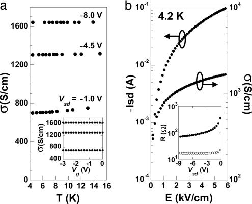
Fig. 2.
Low-temperature device characteristics. (a) Conductivity vs. temperature at varying Vsd for a device cooled beforehand from room temperature to 4.2 K while holding the gate bias constant at Vg = −3 V. (Inset) The conductivity vs. Vg at 4.2 K. (b) Current (and conductivity) vs. source–drain electric field for the same device shown in a, at 4.2 K. (Inset) The channel (filled circles) and contact (open circles) resistance vs. Vsd at 4.2 K.

