Abstract
We present scanning tunneling microscopy (STM) images of single-layer graphene crystals examined under ultrahigh vacuum conditions. The samples, with lateral dimensions on the micrometer scale, were prepared on a silicon dioxide surface by direct exfoliation of crystalline graphite. The single-layer films were identified by using Raman spectroscopy. Topographic images of single-layer samples display the honeycomb structure expected for the full hexagonal symmetry of an isolated graphene monolayer. The absence of observable defects in the STM images is indicative of the high quality of these films. Crystals composed of a few layers of graphene also were examined. They exhibited dramatically different STM topography, displaying the reduced threefold symmetry characteristic of the surface of bulk graphite.
Keywords: two-dimensional, graphite, nanoscience
Since the first reports of experiments on stand-alone, single-layer graphene crystals, (1) this remarkable two-dimensional material has attracted great scientific interest (2–5). There are two alternative approaches for producing graphene layers. In the first method, sample layers are mechanically exfoliated from bulk graphite crystals; in the second method, a surface, such as silicon carbide, is “graphitized” under vacuum conditions (6, 7). The strength of interaction between the underlying substrate and the graphene film is an issue of importance in the study of these materials of monolayer thickness. Very recent results using angle-resolved photoemission spectroscopy (7, 8) on single- and few-layer graphene samples have, for example, shown that interactions between a graphene film and a SiC substrate can be considered weak. On the other hand, several earlier scanning tunneling microscopy (STM) studies of graphitized surfaces, such as Ir(1 1 1) (9), Pt(1 1 1) (10, 11), and SiC (6), also have been performed. In these experiments, the structure observed by STM was strongly influenced by the interaction between the graphitic layer and the underlying substrate, and features unambiguously associated with the electronic properties of an isolated graphene layer could not be identified. The purported differences in the strength of the graphene–substrate coupling may reflect different sample preparation methods and/or various sensitivities of the STM and angle-resolved photoemission spectroscopy techniques to these interactions.
Here we present results of an STM study of single-layer graphene films prepared by mechanical exfoliation and probed on an insulating substrate. For these micrometer-sized samples, the STM topographic images show the hexagonally symmetric honeycomb structure expected for an ideal, unperturbed graphene crystal. STM images for multilayer graphene films prepared in the same fashion display the reduced, threefold symmetry characteristic of the surface of bulk graphite crystals. In addition to the local atomic-scale structure of single-layer graphene samples, we present measurements on the film's topography over the 100-nm length scale. Height variation on the order of 1 nm is observed. These investigations confirm the possibility of preparing high-quality graphene specimens, because atomically resolved STM images of portions of this sample showed no evidence of defects or dislocations in the graphene crystallographic structure. We note that the samples were produced under ambient conditions and then subjected to microfabrication processing and exposure to various organic solvents. The fact that the films survived these severe conditions suggests that graphene holds promise not only for elegant scientific experiments but also for novel electronic devices and sensors.
Results and Discussion
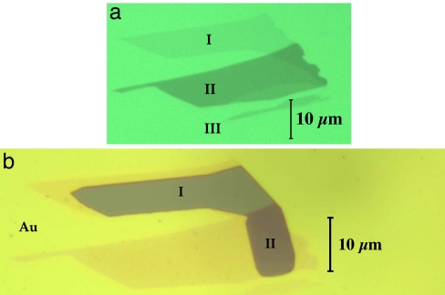
An optical image of the flake used in the experiments described below is shown in Fig. 1a. A region with single-layer graphene (Fig. 1a, I) is visible on top of the wafer surface (Fig. 1a, III). Part of this flake (Fig. 1a, II) exhibits a higher optical density. We estimate this region to have a thickness of five graphene layers. The fabrication and identification of single- and multilayer graphene samples by Raman scattering spectroscopy are described below. Fig. 1b shows an optical image of the sample after electrode deposition around the flake. Most of the single-layer region (Fig. 1b, I) and a portion of the multilayer region (Fig. 1b, II) are accessible for STM studies; the rest of the flake is buried beneath the gold film. Because the thin gold film is partially transparent, the contour of the entire flake of Fig. 1a can still be seen.
Fig. 1.
Optical microscopy images of the graphene flake examined in this study. (a) An image of the sample before deposition of the electrode. Three regions with different optical densities can be identified: I, single-layer graphene; II, multilayer graphene; and III, the silicon-dioxide-coated substrate. (b) An image of the same flake after the deposition of an 18-nm layer of gold. The gold electrode completely covers the substrate and partially covers the graphitic flake. The darker region is the uncovered part.
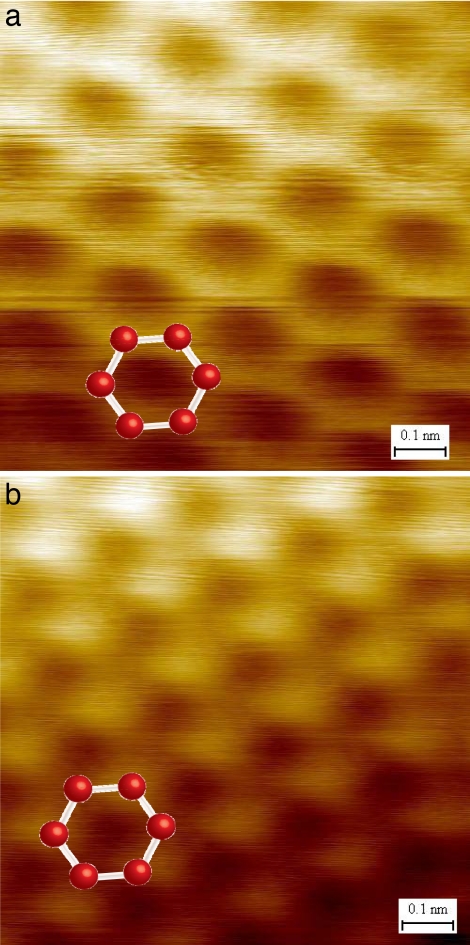
Several hundred images were recorded for different positions of the STM tip. The graphene sample was found to be highly conductive so that tunneling occurs only between the STM tip and the graphene. Thus, the graphene itself and the gold electrode attached to the fringe of the flake (Fig. 1b) provide a return path for electrons in these experiments. In the measurements, the bias was set at a +1-V sample potential (STM images became unstable at low-bias voltages), and a tunneling current of 1 nA was chosen. In the regions that were identified as consisting of single-layer graphene, a honeycomb structure was observed. Fig. 2a shows such an image over a 1-nm2 area. No atomic defects were found in our images, which indicates the high quality of the graphene films produced by the present technique. For comparison, an example of a 1-nm2 image recorded on a multilayer flake is shown in Fig. 2b. The characteristic features of the STM images of Fig. 2 are readily interpreted in terms of the A–B stacking of the graphene planes in graphite. In bulk graphite, the carbon atoms on the surface are not equivalent. Half of the carbon atoms in the surface layer are located above carbon atoms in the adjacent, lower layer (A-type atoms); the other half are sitting over a void (B-type). This asymmetry in the surface atom electronic environment results in a threefold symmetry (“three-for-six”) pattern in which three bright or dark features can be observed for each set of six carbon atoms, consistent with the structure shown in Fig. 2b (12, 13). This behavior also is present for graphene flakes that are two or more atomic layers thick (E.S., D. Stolyarov, Y. Zhang, M. Han, M. Hybertsen, P.K., and G.W.F., unpublished data). For single-layer sheets of graphene, this asymmetry is removed. Consequently, all surface carbon atoms are identical, and a symmetrical honeycomb structure is observed in the STM image. Lattice defects, point-like interactions with the underlying substrate, or folding of the single-layer graphene sheet would be expected to cause significant perturbation of the local electron density and, thus, be reflected in the STM topography. None of these possible features were observed in the present study over the region of the sample investigated under atomically resolved STM.
Fig. 2.
STM topographic images of different regions of the graphene flake of Fig. 1. The images were obtained with Vbias = +1 V (sample potential), I = 1 nA, and a scan area of 1 nm2. A model of the underlying atomic structure is shown as a guide to the eye. (a) Image from a single layer of graphene (region I of Fig. 1). A honeycomb structure is observed. (b) Image of the multilayer portion of the sample (region II of Fig. 1). The characteristic three-for-six STM image of the surface of bulk graphite is observed.
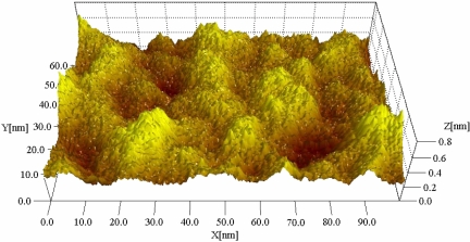
It has been argued theoretically that perfectly flat, two-dimensional crystals are not stable (14). Indeed, a very recent transmission electron microscopy experimental study has demonstrated nanometer scale structural deformations in free-standing graphene films (15). To examine mesoscopic graphene structures as formed on an insulating substrate, the large-scale topography of the present sample was investigated. A stereoscopic, large-area (100 × 62 nm) STM image of a single-layer graphene sheet (from region I of Fig. 1) is shown in Fig. 3. This image has been corrected by using plane height offset obtained from a second-degree line mean square fitting routine. In Fig. 3, the vertical scale is enlarged to highlight the details of the graphene “landscape.” Although roughness beyond the atomic level is obviously present, the characteristic fluctuation in height is relatively modest. The observed height variation of ≈0.5 nm, which occurs on a lateral scale of ≈10 nm, is comparable with that measured by atomic force microscopy for similar graphene samples before microprocessing for the electrode deposition. The height variation is also comparable with that determined separately by atomic force microscopy for the underlying silicon dioxide surface (online supporting materials of ref. 1). Consequently, the observed nonperiodic roughness may arise simply from the graphene film following (at least partially) the features of the underlying silicon dioxide surface. In addition, transmission electron microscopy studies of suspended graphene films have demonstrated that free-standing graphene films are corrugated on a mesoscopic scale, with out-of-plane deformations up to 1 nm (15). Of course, STM probing is accompanied by the application of elastic forces on the graphene sample (12). Single-layer graphene sheets are especially susceptible to deformation resulting from such forces, which also may contribute to the observed large-scale topography.
Fig. 3.
Stereographic plot of a large-scale (100 × 62 nm) STM image of a single-layer graphene film on the silicon dioxide surface. The STM scanning conditions were Vbias = 1 V (sample potential) and I = 0.6 nA. The 0.8-nm scale of the vertical (Z) coordinate is greatly enlarged to accentuate the surface features.
Conclusions
Single-layer graphene flakes isolated on a silicon dioxide surface have been identified and distinguished from multilayer flakes by using Raman scattering. Ultrahigh vacuum STM images of both single- and multilayer flakes have been observed. Whereas multilayer flakes exhibit STM images with threefold symmetry typical of bulk graphite, single-layer graphene crystals display a symmetric honeycomb structure in which all of the surface atoms contribute equally to the tunneling images. Our STM studies demonstrate that single-layer samples of graphene prepared by mechanical exfoliation exhibit a high degree of crystalline order and only subnanometer fluctuations in height on a longer lateral scale. Remarkably, these favorable material properties persist despite the relatively harsh processing conditions used to prepare the samples. Furthermore, the single-layer graphene crystals, as gauged by the atomically resolved STM topography, show no prominent signs of perturbation induced by interaction with the underlying substrate. These materials are thus well suited for advancing both the science and technology of highly two-dimensional systems.
Materials and Methods
Sample Fabrication.
The graphene films for this study were prepared by the mechanical exfoliation of bulk Kish graphite (Toshiba Ceramics, San Jose, CA) according to the procedure reported in ref. 1. The exfoliated graphitic flakes were deposited on the surface of a silicon wafer covered by a 300-nm-thick silicon dioxide film. Graphene flakes of monolayer thickness were initially selected from the vast majority of thicker ones by visual inspection with an optical microscope.
Electrical contact to the graphene was obtained by depositing gold electrodes around the flake by using electron beam lithography. All nonconductive silicon dioxide regions of the surface were covered by a layer of gold because accidental positioning of the STM tip on an insulating region caused a tip crash and permanent tip damage. The typical procedure for microfabrication of this structure was performed by spin-casting a two-layer resist of methylmethacrylate/methacrylic acid copolymer (first layer; MicroChem, Newton, MA) and 950K poly(methyl methacrylate) (second layer; MicroChem). Resist around and at the edges of the flake was removed by electron beam exposure with a scanning electron microscope (FEI, Hillsboro, OR) followed by development in methyl isobutyl ketone/isopropanol at a 1:3 ratio. A metal film (1-nm Cr/18-nm Au) was then deposited with an electron-beam evaporator (model no. SC2000; Semicore, Livermore, CA). The metal film present above the graphene flake was removed by lift-off of the underlying resist in acetone. The roughness of this resulting graphene film did not exceed 1.5 nm, as measured by atomic force microscopy. The area of the gold electrode created by this method was ≈500 μm2. As a last step, a further layer of gold (150 nm) was deposited on uncovered areas of the wafer by using a shadow mask. This film provided good mechanical and electrical contact between the graphene crystal and the STM sample holder.
Raman Spectroscopy.
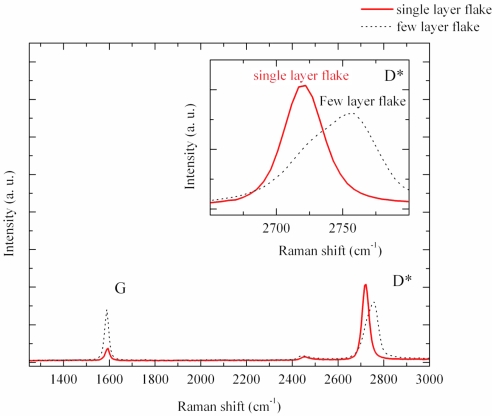
Recently it has been shown that Raman spectroscopy is a reliable, nondestructive tool for the identification of single- and multilayer graphene samples (16, 17). Before the present STM studies, the graphene sample shown in Fig. 1b was characterized with Raman spectroscopy. These Raman measurements were performed with a microscope set-up in the backscattering geometry under ambient conditions at room temperature. The output of an Ar ion laser (457.9 nm) was focused to a spot size of ≈1 μm2 to permit different spatial regions of the graphene sample to be probed. The laser spot could be positioned on the sample to an accuracy of a few hundred nanometers. The dependence of the Raman scattering on laser power was examined to ensure that the graphene flake was not heated or damaged by the incident laser beam. Fig. 4 shows the Raman spectrum of single-layer graphene (Fig. 1b, I) and of a few-layer flake (Fig. 1b, II) in the spectral region of the graphite G and D* modes. Gold electrodes, located a few micrometers away from the region under study, do not contribute to the Raman signal. The D* mode is the second-order optical phonon mode near the K point in the graphene Brillouin zone; it is particularly strong because of its double-resonant enhancement in the Raman process. The change in the electronic structure in going from single-layer graphene to two or more layers is most easily identified in the D* mode, because this mode changes from a narrow and symmetric feature to one exhibiting an asymmetric line shape on the high-energy side (16). This behavior is observed in the Raman spectra shown in Fig. 4, demonstrating that region I is indeed a single-layer flake, whereas region II consists of several graphene layers. The increase of the G-band intensity going from single-layer to few-layer regions of the sample further supports this assignment (17). Raman spectral patterns were repeatable at different spots in each region of the sample.
Fig. 4.
Comparison of Raman spectra at 457.5 nm for single-layer (solid line) and multilayer (dashed line) regions of the graphitic flake described in Fig. 1. The two intense features are the G peak at a Raman shift of ≈1,580 cm−1 and the D* band at ≈2,710 cm−1. The D* band (enlarged in Inset) of a few-layer flake is blue-shifted and broadened with respect to that of the single-layer graphene sample. Moreover, the D* peak of single-layer graphene is symmetric, whereas the D* band corresponding to the multilayer sample has a complex asymmetric shape.
STM Measurements.
Sample imaging was performed with a low-temperature STM (model LT-STM; Omicron NanoTechnology, Taunusstein, Germany) at liquid nitrogen temperature. The measurements were performed under ultrahigh vacuum at a background pressure of <1.5 × 10⁻¹⁰ torr (1 torr = 133 Pa). After the sample was moved into the ultrahigh vacuum chamber, it was annealed at 280°C for 6 h to remove the resist residue and other contaminants. An etched tungsten tip, also annealed before imaging, was used to obtain the STM topographs. The images were analyzed with the SPIP, version 4.4.6.0, software package (Image Metrology, Hørsholm, Denmark). The images represent raw STM topographs and have not been modified unless otherwise indicated. The algorithm that allows a flake to be found and regions within the flake to be identified is similar to the method described in our previous work (E.S., D. Stolyarov, Y. Zhang, M. Han, M. Hybertsen, P.K., and G.W.F., unpublished data). Briefly, the STM tip is positioned close to the flake by using a telescope. After an initial landing, the STM is moved step-by-step with respect to the sample, and the surface is imaged after each step. The gold-flake boundary could be readily found and served as a reliable marker of the STM tip position. By using the optical image of the flake as a map, an unambiguous correspondence was established between the local STM images and the macroscopic position of the STM tip.
Acknowledgments
We thank Etienne De Poortere, Kirill Bolotin, and Melinda Han for invaluable help in the microfabrication of the samples used in this study. This work was supported by National Science Foundation Grant CHE-03-52582 (to G.W.F.); Major Research Instrumentation Program Grant CHE-04-21191; Nanoscale Science and Engineering Centers Program Grant CHE-06-41523; the New York State Office of Science, Technology, and Academic Research; and U.S. Department of Energy Grants DE-AC02-98CH10886 (to M.S.H.) and DE-FG02-03ER15463 (to T.F.H.).
Abbreviation
- STM
scanning tunneling microscopy.
Footnotes
The authors declare no conflict of interest.
References
- 1.Novoselov KS, Geim AK, Morozov SV, Jiang D, Zhang Y, Dubonos SV, Grigorieva IV, Firsov AA. Science. 2004;306:666–669. doi: 10.1126/science.1102896. [DOI] [PubMed] [Google Scholar]
- 2.Heersche HB, Jarillo-Herrero P, Oostinga JB, Vandersypen LMK, Morpurgo AF. Nature. 2007;446:56–59. doi: 10.1038/nature05555. [DOI] [PubMed] [Google Scholar]
- 3.Zhang Y, Jiang Z, Small JP, Purewal MS, Tan YW, Fazlollahi M, Chudow JD, Jaszczak JA, Stormer HL, Kim P. Phys Rev Lett. 2006;96:136806. doi: 10.1103/PhysRevLett.96.136806. [DOI] [PubMed] [Google Scholar]
- 4.Zhang YB, Tan YW, Stormer HL, Kim P. Nature. 2005;438:201–204. doi: 10.1038/nature04235. [DOI] [PubMed] [Google Scholar]
- 5.Novoselov KS, Geim AK, Morozov SV, Jiang D, Katsnelson MI, Grigorieva IV, Dubonos SV, Firsov AA. Nature. 2005;438:197–200. doi: 10.1038/nature04233. [DOI] [PubMed] [Google Scholar]
- 6.Berger C, Song Z, Li X, Wu X, Brown N, Naud C, Mayou D, Li T, Hass J, Marchenkov AN, et al. Science. 2006;312:1191–1196. doi: 10.1126/science.1125925. [DOI] [PubMed] [Google Scholar]
- 7.Ohta T, Bostwick A, Seyller T, Horn K, Rotenberg E. Science. 2006;313:951–954. doi: 10.1126/science.1130681. [DOI] [PubMed] [Google Scholar]
- 8.Bostwick A, Ohta T, Seyller T, Horn K, Rotenberg E. Nat Phys. 2007;3:36–40. [Google Scholar]
- 9.Klusek Z, Kozlowski W, Waqar Z, Datta S, Burnell-Gray JS, Makarenko IV, Gall NR, Rutkov EV, Tontegode AY, Titkov AN. Appl Surf Sci. 2005;252:1221–1227. [Google Scholar]
- 10.Land TA, Michely T, Behm RJ, Hemminger JC, Comsa G. Surf Sci. 1992;264:261–270. [Google Scholar]
- 11.Ueta H, Saida M, Nakai C, Yamada Y, Sasaki M, Yamamoto S. Surf Sci. 2004;560:183–190. [Google Scholar]
- 12.Magonov S, Whangbo M. Surface Analysis with STM, AFM: Experimental and Theoretical Aspects of Image Analysis. New York: VCH; 1996. [Google Scholar]
- 13.Sinitsyna OV, Yaminsky IV. Uspekhi Khimii. 2006;75:27–35. [Google Scholar]
- 14.Mermin ND. Phys Rev. 1968;176:250–254. [Google Scholar]
- 15.Meyer JC, Geim AK, Katsnelson MI, Novoselov KS, Booth TJ, Roth S. Nature. 2007;446:60–63. doi: 10.1038/nature05545. [DOI] [PubMed] [Google Scholar]
- 16.Ferrari AC, Meyer JC, Scardaci V, Casiraghi C, Lazzeri M, Mauri F, Piscanec S, Jiang D, Novoselov KS, Roth S, et al. Phys Rev Lett. 2006;97:187401. doi: 10.1103/PhysRevLett.97.187401. [DOI] [PubMed] [Google Scholar]
- 17.Gupta A, Chen G, Joshi P, Tadigadapa S, Eklund PC. Nano Lett. 2006;6:2667–2673. doi: 10.1021/nl061420a. [DOI] [PubMed] [Google Scholar]


