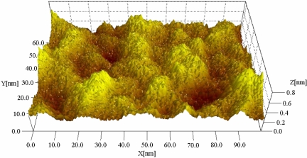
Fig. 3.
Stereographic plot of a large-scale (100 × 62 nm) STM image of a single-layer graphene film on the silicon dioxide surface. The STM scanning conditions were Vbias = 1 V (sample potential) and I = 0.6 nA. The 0.8-nm scale of the vertical (Z) coordinate is greatly enlarged to accentuate the surface features.

