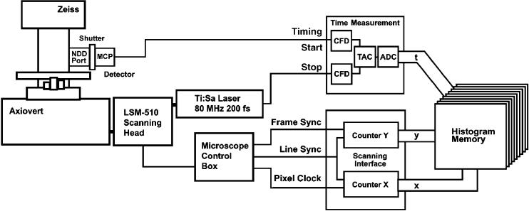
Fig. 1.
A schematic illustration of the multi-dimensional TCSPC microscope. The recording electronics consists of a time measurement channel, a scanning interface and a large histogram memory. The time measurement channel contains the usual TCSPC building blocks. Two constant fraction discriminators, CFD, receive the single photon pulses from the detector and the reference pulses from the laser. The time-to-amplitude converter, TAC, measures the time from the detection of a photon to the next laser pulse. The analog-to-digital converter, ADC, converts the TAC output voltage into an address for the memory. The scanning interface is a system of counters. It receives the scan control pulses from the microscope and determines the current position of the laser beam in the scanning area. When a photon is detected the device determines the time, t, within the fluorescence decay curve and the location of the laser spot within the scanning area, x,y. These values are used to address the histogram memory. Consequently, in the memory the photon distribution vs. t, x and y builds up. The result can be interpreted as a stack of images for different times after the excitation pulse or as an array of pixels containing a complete fluorescence decay function each.

