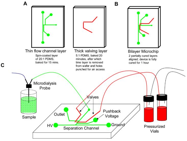
Figure 1.

Fabrication steps used in these studies. A) 2 separate masters are used; 1 with the flow channel design and 1 with the valving layer design. The flow channel layer is spin coated and partially cured. The valving layer is 3.5 mm thick and also partially cured. B) The valving layer is removed from the wafer, aligned over the flow channel layer, and both layers are fully cured. C) The microchip device is connected to tubing that leads to either the microdialysis probe or pressurized actuation vials.
