Abstract
A fully integrated, wireless neural interface device is being developed to free patients from the restriction and risk of infection associated with a transcutaneous wired connection. This device requires a hermetic, biocompatible encapsulation layer at the interface between the device and the neural tissue to maintain long-term recording/stimulating performance of the device. Hydrogenated amorphous silicon carbide (a-SiCx:H) films deposited by a plasma enhanced chemical vapor deposition using SiH4, CH4, and H2 precursors were investigated as the encapsulation layer for such device. Si-C bond density, measured by Fourier transform infrared absorption spectrometer, suggests that deposition conditions with increased hydrogen dilution, increased temperature, and low silane flow typically result in increase of Si-C bond density. From the variable angle spectroscopic ellipsometry measurement, no dissolution of a-SiCx:H was observed during soaking tests in 90°C phosphate buffered saline. Conformal coating of the a-SiCx:H in Utah electrode array was observed by scanning electron microscope. Electrical properties were studied by impedance spectroscopy to investigate the performance of a-SiCx:H as an encapsulation layer, and the results showed long term stability of the material.
Keywords: amorphous silicon carbide, biomedical device encapsulation, dielectrics, PECVD, passivation
1. Introduction
Development of a neural interface device, to help fully or partially paralyzed patients, has been pursued for decades [1–3]. The ultimate goal of neural interface is to sense and stimulate neural action potentials to receive and send information from the nervous system, respectively. One of the most promising neural interface architectures is a device combining silicon micromachined electrode arrays, Utah electrode array [4, 5], with an integrated circuit shown in Fig. 1 [6], due to its potential for freeing the patient from the restriction and risk of infection of a wired connection. In order to maintain long-term recording and/or stimulating performance of the device, a biocompatible encapsulation layer is required at the interface between the device and the body tissue. Besides being biocompatible, the encapsulation layer needs to have the following properties in order to be used on the chronic neural recording and stimulating electrode array.
Fig 1.
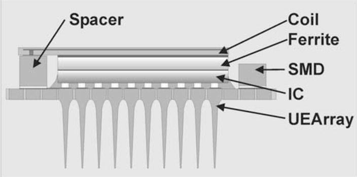
Schematic of the integrated, wireless neural interface device. This device comprises a Utah Electrode Array (UEA), surface mounted devices (SMD), integrated circuit (IC), a coil and ferrite. Underfiller is used in between interconnections. The whole device must be encapsulated except active electrode tip site.
Hermetic encapsulation: The coating needs to be pinhole free and adhere well to all the surface materials of the device—to isolate the integrated device from rigorous physiological environment, such that device degradation or corrosion can be prevented.
Conformal coating: Uniform coating allows uniform protection while keeping array geometry intact after encapsulation.
High electrical resistivity: High resistivity of the coating electrically isolates the individual neural electrodes.
Low dielectric constant: Parasitic losses, cross-talk, and frequency modulation due to resistive-capacitive components coupling can be reduced with a low dielectric constant encapsulation.
Low temperature deposition process: Deposition temperature lower than 200°C is required to avoid the degradation of the integrated device.
It is difficult to find an ideal material that satisfies all these characteristics for chronic implantation. Therefore, if a material provides the protection ensuring a functional implanted device during the designed life time in physiological environment, it is considered to be the biocompatible encapsulation material; for example, Parylene [7–9] and silicon nitride [7]. However, silicon nitride has been found to dissolve in the physiological environment, whereas the adhesion of Parylene to inorganic materials without proper surface treatment has been less satisfactory [8, 10].
Crystalline silicon carbide is known for its high values of hardness ( 9 on Mohs hardness scale) and chemical inertness. The strong Si-C chemical bonds are responsible for inert characteristics of SiC [11]. a-SiCx:H has low dielectric constant (4.4–4.9) and low moisture intake [12, 13], thereby satisfies two conditions needed for a device encapsulation layer. Due to the controllable electrical and optical properties, a-SiCx:H has been investigated intensely in the fields of optoelectronics [14, 15], solar cell technology [16], and surface passivation [17, 18]. However, the use of a-SiCx:H as the biomedical device coating has gained attention only recently. For example, Bolz et al. used doped a-SiCx:H as a bioactive coating material of stent implants to improve hemocompatibility [19, 20]. Kalnins et al. implanted a-SiCx:H coated stents into one hundred patients and suggested that a-SiCx:H can reduce thrombosis and restenosis rate after angioplastry [21]. Cogan et al. demonstrated that a-SiCx:H has desirable dielectric property to insulate the neuroprobe from moisture and ionic species [7].
However, the study of a-SiCx:H deposition process to fulfill the encapsulation requirements on the biomedical device has not yet been explored. In this research, we evaluated a-SiCx:H as the biocompatible, hermetic, and electrically insulating coating for the silicon-based integrated device; a-SiCx:H deposition conditions versus film properties were studied for performance optimization.
To avoid degradation of the integrated device during the coating process, we focused on a low temperature (150°C–275°C) plasma enhanced chemical vapor deposition (PECVD) process. Previously, most PECVD a-SiCx:H studies have been conducted at a deposition temperature between 250°C and 400°C and at such temperatures, the polymeric underfiller material used in the integrated wireless device to relieve inter-chip stress is degraded. For the current architecture, it is necessary to develop a process with the deposition temperature lower than 200°C. Most SiC films deposited by PECVD have an amorphous structure without long-range periodic order. Pereyra et al. have suggested that the Si-C bond density is a function of hydrogen dilution and silane ratio in PECVD process, and highly ordered a-SiCx:H is possible [22]. This work explored the process to grow silicon carbide of different Si-C bond densities at different temperatures, and compared their encapsulation properties and performances. In this paper we show that low stress, low dielectric constant, high Si-C bond density, and pinhole free a-SiCx:H film can be deposited at low temperature (<=200°C).
2. Experimental Details
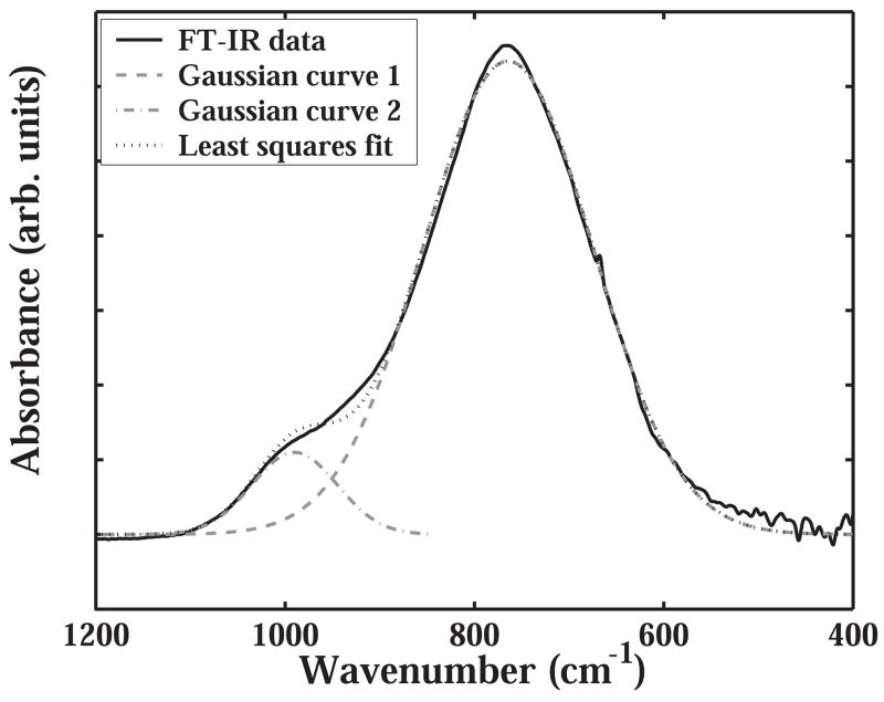
a-SiCx:H films were deposited by PECVD (MVSystems Inc., Golden, Colorado, USA) using a 13.56 MHz RF generator to drive the plasma, and a electrode spacing of 2.3 cm. Hydrogen was used as dilution gas source, and silane (SiH4) and methane (CH4) were used as Si and C precursors, respectively. Deposition pressure and power were fixed at 400 mTorr and 0.25 watts cm−2, respectively. The precursor ratio, defined as SiH4/(SiH4+CH4), and hydrogen dilution, defined as H2/(SiH4+CH4), are gas flow ratios that have significant influence on film properties and are therefore controlled. In this work, there are mainly two sets of deposition conditions, one is defined as ‘silane starving’ when precursor ratio =0.17, and the other is defined ‘non-silane-starving’ when precursor ratio =0.29. By varying the precursor ratio, the hydrogen dilution, and the substrate temperature (Ts), a-SiCx:H films were deposited on silicon substrates and subsequently characterized. The film’s bonding structure was studied on a double-side polished wafer with a Fourier transform infrared (FT-IR) absorption spectrometer operating in transmission mode. In all the absorption spectra, thickness was normalized and the absorption of silicon substrate as well as the influences of interference was taken into account. The relative Si-C bond density was calculated by integrating the absorption intensity in deconvoluted absorption curve of the FT-IR spectrum. The deconvolution of FT-IR data (Fig. 2) was done by fitting Gaussian curves using the least square method available in Matlab® v7.2 (The Mathworks, Inc. MA, USA).
Fig. 2.
The sum of integrals of the two Gaussian curves was to fit the experimental FT-IR data within the chosen wavenumber limits. The peak at 750 cm−1 is associated with Si-C bond stretching and the peak at 1000 cm−1 is associated with Si-(CH)n bond wagging and rocking.
Silicon substrates deposited with a-SiCx:H were placed into 90°C phosphate buffered saline (PBS) solution (pH=7.4) to investigate the dissolution rate and defect density of the films. A variable angle spectroscopic ellipsometry system ( J.A. Woolam Co., Inc., Lincoln, NE. USA) was used to measure the refractive index and thickness of the a-SiCx:H film before and after the PBS soaking tests. A Cauchy model was fitted to delta and psi to determine the refractive index and thickness of the films. Curvature deflection of the silicon substrate after a-SiCx:H deposition was measured by a surface profiler (KLA-Tencor P-10, San Jose, CA. USA) to calculate film stress. From the measured change in radius of curvature, the corresponding film stress σf is calculated by using the modified Stoney equation (1909):
| (1) |
where the substrate thickness is given by ds, thin film thickness is given by df, Young’s modulus is given by E, and Poisson’s coefficient is given by ν. R1 and R2 is the radius of curvature before and after thin film deposition, respectively.
Utah electrode array was encapsulated with a-SiCx:H and embedded into acrylic resin, followed by a polishing process to expose the array cross section. The conformity and coating uniformity on the Utah electrode array (UEA) was evaluated by the scanning electron microscope (SEM). A Schottky field emission source with 5 keV beam energy and a secondary electron detector were used in SEM analysis. Carbon paint was used to cover the acrylic resin block except device needle part to avoid charging problem in the image.
The impedance spectroscopy was performed using the interdigitated electrode chips (IDEs). Titanium/Platinum (50 nm/330 nm) IDEs were deposited and patterned on oxidized silicon substrate by standard photolithography using lift-off technique. The Ti and Pt films were sputtered on the substrate sequentially to serve as the adhesive and the conductive layers, respectively. a-SiCx:H was deposited on the IDEs and put into Ringer’s solution for impedance spectroscopy measurement. Long-term (> 6 months) changes in electrical properties of the a-SiCx:H films was monitored weekly by the 50mV alternating current (AC) impedance spectroscopy measurement (Gamry Instruments EIS300, Warminster, PA. USA) where the AC frequency ranged from 1Hz to 105 Hz. Dielectric constant was estimated from the initial impedance and corresponding frequency acquired from impedance spectroscopy spectrum
Results and Discussions
We investigated the influence of temperature, hydrogen dilution and precursor ratio on Si-C bond density, deposition rate and refractive index. The deposition variables and some characterization results are summarized in Table I.
Table I.
Deposition conditions of the a-SiCx:H films and selected characterization results
| Deposition ID SiH4 -CH4 -H2 -Ts | Substrate temperature Ts | [H2] sccm | Precusor ratio | Hydrogen Dilution | Si-C relative bond density ratio | Deposition rate (nm/min) | Refractive Index (η) at 500 nm |
|---|---|---|---|---|---|---|---|
| 2–10–5–275 | 275°C | 5 | 0.17 | 0.36 | 1.00 | 6.8 | 1.90 |
| 2–10–80–275 | 80 | 5.71 | 1.28 | 3.2 | 2.58 | ||
| 2–10–180–275 | 180 | 12.85 | 2.54 | 2.5 | 2.79 | ||
|
| |||||||
| 2–10–5–200 | 200°C | 5 | 0.17 | 0.36 | 0.51 | 7.4 | 1.79 |
| 2–10–20–200 | 20 | 1.42 | 0.77 | 6.6 | 1.82 | ||
| 2–10–80–200 | 80 | 5.71 | 1.02 | 3.2 | 2.32 | ||
| 2–10–180–200 | 180 | 12.85 | 1.97 | 2.6 | 2.72 | ||
|
| |||||||
| 2–10–180–150 | 150°C | 180 | 0.17 | 12.85 | 1.34 | 2.9 | 2.44 |
|
| |||||||
| 4–10–5–275 | 275°C | 5 | 0.29 | 0.36 | 0.77 | 8.9 | 1.96 |
| 4–10–80–275 | 80 | 5.71 | 0.92 | 4.6 | 2.83 | ||
|
| |||||||
| 4–10–5–200 | 200°C | 5 | 0.29 | 0.36 | 0.50 | 7.0 | 1.88 |
| 4–10–80–200 | 80 | 5.71 | 0.79 | 4.4 | 2.47 | ||
|
| |||||||
| 4–10–180–150 | 150°C | 180 | 0.29 | 12.85 | 0.95 | 2.8 | 2.62 |
Due to weaker bond energy of Si-H (70.9 Kcal/mole) than C-H (98.8Kcal/mole), SiH4 molecules are decomposed into reactive free radicals easier than CH4: More silicon radicals than carbon radicals were present in the plasma of low power regime. The majority carbon atoms in the film are incorporated through reacting with silane radicals so that soft graphite-like structure is avoided [23]. In addition, a higher CH4 to SiH4 flow ratio is needed to deposit the film with equivalent Si and C atomic ratio in low power regime[24], and the maximum Si-C bond density has been deposited at about 15% silane in precursor gas [22]. The Si-C bond density (N) can be estimated from integral of FT-IR absorption spectra by means of the following equation 1
| (2) |
where the integral of the absorption spectra α(ω) as a function of frequency (ω) was normalized by the sample thickness. The absorption coefficient is given as A[25]. The deconvoluted curve with peak at 750–780cm−1 is attributed to the absorption from Si-C stretching vibration.
Two different precursor ratios were used to compare their Si-C bond density: silane starving and non-silane starving; and a lower precursor ratio (0.17) yielded a higher Si-C bond density than precursor ratio of 0.29. All the Si-C bond density is compared with the sample deposited at 275°C, precursor ratio of 0.17 and hydrogen dilution of 0.36, and the relative Si-C bond density ratio is listed in Table I.
3.1 Hydrogen dilution effects
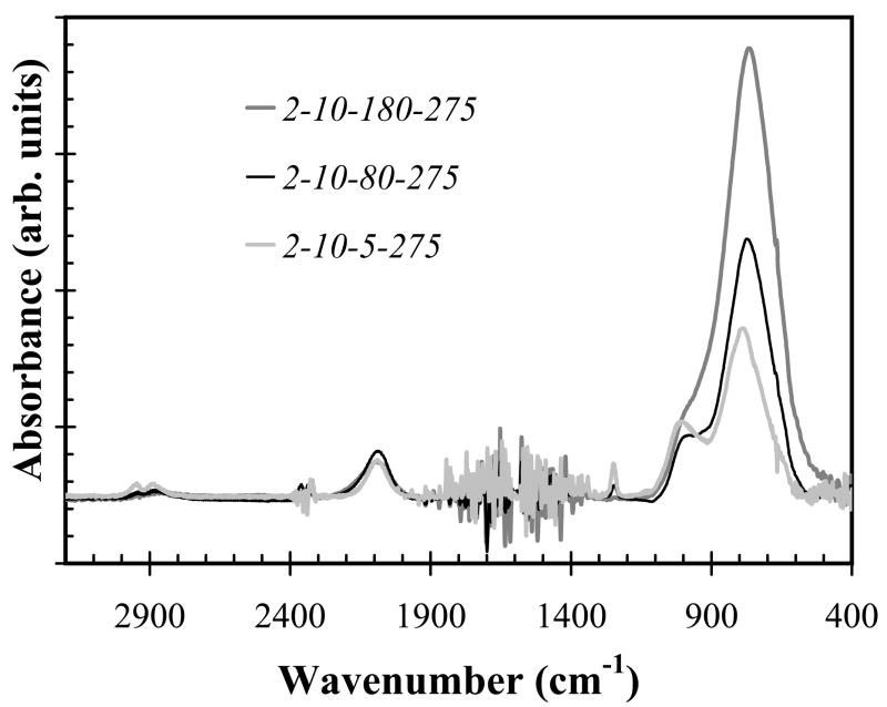
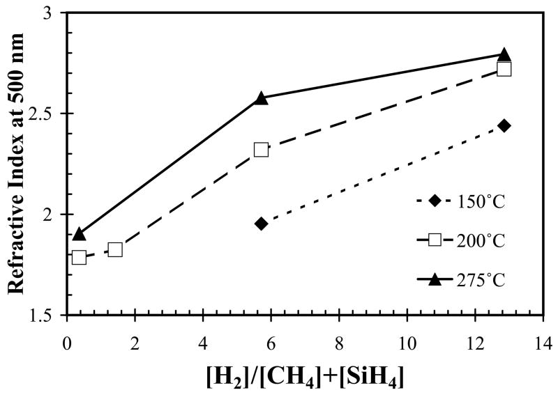
In silane-starving condition (precursor gas flow ratio x=0.17), increasing hydrogen dilution increases Si-C bond density and the refractive index (η), as shown in Fig. 3 (FT- IR plot) and Fig. 4, respectively. The IR absorbance at a given wavenumber represents a specific bond structure, and is proportional to the density of bond absorbing the light when film thickness is normalized. Wavenumber of absorption peak in infrared spectra versus bond assignments were listed in Table II. The absorption noises within the wavenumber range 1300–1900 and 2300–2400 cm−1 come from the background of water and carbon dioxide, respectively, and were therefore ignored. Thus, increase of hydrogen dilution decreased the intensity of infrared absorption band within wavenumber 2800– 3000 cm−1 and increased absorption band at wavenumber of 750–780 cm−1 (Fig. 3), indicating the decrease of CHn groups density and increase of Si-C bond density, respectively. The refractive index, measured by ellipsometry, increased from as low as 1.75 to as high as 2.83, as hydrogen dilution ratio and temperature were increased (Fig. 4). The refractive index of bulk single crystal 3C-SiC is approximately 2.55.
Fig. 3.
Infrared absorption spectra from a-SiCx:H samples deposited with precursor ratio 0.17 and deposition temperature 275°C, and hydrogen flow varied from 5 sccm to 180 sccm (hydrogen dilution of 0.36 –12.85).
Fig. 4.
Refractive index of a-SiCx:H films on silicon substrates plotted as a function of hydrogen dilution and substrate temperature during deposition.
Table II.
Absorption peak wavenumber in Infrared spectra versus bonding configuration assignment
It has been suggested that CHn groups terminate the silicon-carbon network structure and form micro-voids: The higher infrared absorption within wavenumber 2800–3000 cm−1 (CHn stretching modes) indicate higher presence of CHn groups, and thus a more porous and lower refractive-index film [15, 23]. It has been proposed that increasing the hydrogen dilution reduces the CHn content in the film by hydrogen preferential etching the carbon bonds [22]. We propose the other possibility that the hydrogen may remove methyl radicals as methane–both hypotheses explain the observation that a higher hydrogen dilution results in less absorption from CHn bands.
With non-silane-starving condition (precursor ratio of 0.29), the increase of the hydrogen dilution and temperature resulted in the same trend of increase of the refractive index as with silane starving condition. However, the availability of silane in the plasma may promote the formation of a random bonding structure rather than preferred hetero-nuclear (Si-C) bond [22], and thus, relative lower Si-C bond density compared to silane starving as indicated in Table I.
3.2 Temperature effect
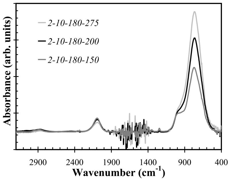
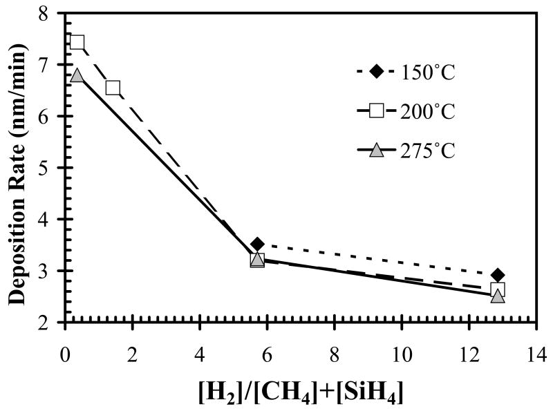
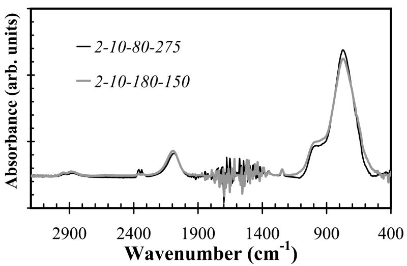
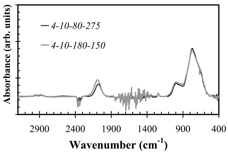
Using silane starving deposition conditions (precursor ratio=0.17), as the substrate temperature increased, both the refractive index of a-SiCx:H films and Si-C absorption band intensity increased as shown in Fig. 4 and Fig. 5, respectively. However, the increased temperature had little effect on the deposition rate, as shown in Fig. 6, by the closely overlapping deposition rates for all temperatures. Also note that the change of SiC density as temperature reduced can be compensated by increasing hydrogen dilution, in other words, we can decrease temperature while increasing hydrogen dilution to get identical or similar FT-IR spectrum as shown in Fig. 7a and Fig. 7b.
Fig. 5.
FT-IR absorption spectra for samples deposited with a constant precursor ratio of 0.17 and hydrogen dilution of 12.85, while the substrate temperature was varied from 150°C to 275°C. Increasing temperature increased Si-C absorption band intensity (wavenumber of 750 cm−1 ).
Fig. 6.
The deposition rate plotted as a function of H2 dilution ratio and temperature. Samples were deposited with a constant precursor ratio of 0.17.
Fig. 7.
Fig. 7a and 7b. FT-IR spectra for both silane starving (a) or non-starving (b) condition, at the deposition temperature of 150°C and 275°C while increasing hydrogen flow from 80 sccm to 180 sccm, FT-IR spectrum of the samples showed almost identical Si-C bond absorbance intensity.
3.3 Film Stress
High film stress can cause the a-SiCx:H film to delaminate or crack, which compromises the encapsulation provided by the film. Windischmann et al. have reported that a-SiCx:H grown at temperatures lower than 400°C tended to be under high compressive stress; however, thermal annealing can relieve the residual stress by mechanisms including releasing incorporated hydrogen from the film [28]. In this work, the a-SiCx:H films deposited on silicon substrate at 200°C had a residual biaxial compressive stress, which increased from 130 MPa to 328 MPa as the hydrogen ratio increased from 0.36 to 5.71. The measured film stresses suggested that low temperature and silane-starving processes yielded low stress, and hence high temperature annealing process can be avoided. In addition, films deposited on silicon substrates at 200°C have low stress allowing further increase of the thickness without compromising encapsulation property.
3.4 Soaking test
The encapsulation properties of a-SiCx:H films with different Si-C bond density were tested by soaking the films in 90°C PBS solution over time, and observing the film integrity.
Two failure modes were anticipated for the soaking test: material dissolution and defect generation. Film dissolution was investigated using ellipsometry to measure the film thickness as function of soaking time. Films with poor adhesion and/or pinhole defects allow PBS to penetrate through the encapsulation; the PBS solution was found to generate rectangle or square defects as the PBS attacks the silicon substrate presumably on preferential crystal planes as shown in Fig. 8.
Fig. 8.
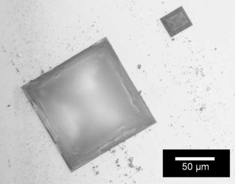
Rectangle or square shape defects resulted from the etching of silicon substrate.
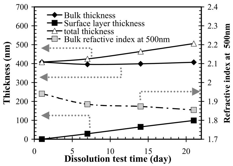
No dissolution was observed by thickness measurements using ellipometry; instead, most of the a-SiCx:H films tended to slightly increase in thickness as shown in Table III.. Refractive index at 500 nm is given as ‘η-500’ and thickness is given as‘t’ in the table. In ellipometry measurement, the data can only be fitted accurately with Delta and Psi measured from the soaked samples by using 2-layer Cauchy model: a lower- refractive-index surface layer and higher-refractive-index bulk layer. The refractive index in the bulk layer of the soaked sample was very close to that of pre-test sample; the lower refractive index in surface layer than that at bulk a-SiCx:H film may due to a rough and oxidized surface grew during the test (Fig. 9 and Table III). Irrespective of the mechanism of the changes in surface properties, the small increase in total thickness over time is acceptable for chronic encapsulation.
Table III.
Summary of a-SiCx:H films thickness changes during soaking test.
| Deposition ID | Thickness change (%)after soaking | Prior to soaking test | After 3–6 weeks soaking | ||||
|---|---|---|---|---|---|---|---|
| t (nm) | η-500 | t-bulk | η-500 bulk | t- surface | η-500 surface | ||
| 2–10–5–275 | 24% (3wks) | 408 | 1.90 | 407 | 1.86 | 99 | 1.26 |
| 2–10–80–275 | 13% (4wks) | 421 | 2.58 | 402 | 2.55 | 72 | 1.13 |
| 4–10–80–275 | 12.4%(4wks) | 556 | 2.83 | 546 | 2.85 | 79 | 1.17 |
|
| |||||||
| 2–10–20–200 | 13.5%(4wks) | 786 | 1.82 | 789 | 1.81 | 103 | 1.02 |
| 2–10–80–200 | 6.6%(6wks) | 639 | 2.43 | 667 | 2.41 | 47 | 1.29 |
|
| |||||||
| 4–10–80–150 | 0.1%(3 wks) | 729 | 2.06 | 649 | 2.20 | 85 | 1.49 |
Fig. 9.
Thickness as a function of soaking time for the sample deposited at 275°C, precursor ratio of 0.17, and hydrogen dilution of 0.36. The overall film thickness (bulk thickness + surface thickness) increased as a function of the soaking time.
a-SiCx:H films deposited at low hydrogen dilution (5 sccm), low temperature (<200°C), and non-silane starving were found by FT-IR to have low Si-C bond density and low refractive index (indicating porosity); and these films were easily scratched by a scalpel. In addition, these films suffered from large quantities of square defects after 1 week PBS soaking test. These results suggest that a low Si-C bond density and porous film may provide little protection in saline solution. Films with high Si-C bond density but very thin film thickness were also compromised early in soaking tests. The films deposited at 200°C using a precursor ratio of 0.17 and a hydrogen dilution of 5.71, but different thicknesses of 380 nm and 650 nm were subjected to the soaking test and compared. Many square defects were generated on the 380 nm-thick film after a 2-week-soaking test, whereas the 650 nm-thick film remained intact after a 6-week soaking test.
3.5 Impedance Spectroscopy
Based on the soaking test results, 650 nm thick a-SiCx:H was deposited on Ti/Pt interdigitated electrode test structure (Fig. 10) for impedance spectroscopy characterization. These films were deposited at 200°C using a precursor ratio of 0.17 and hydrogen dilution of 5.71 to minimize stress and investigate the film electrical properties. Compared to leakage current test, impedance spectroscopy reveals the impedance over a frequency range of 1 Hz to 105 Hz, and is a more sensitive method to monitor the change of the electrical property of encapsulation.
Fig. 10.

IDE structure for Impedance spectroscopy test. The width of spacing as well as the interdigitated electrodes was 130 μm.
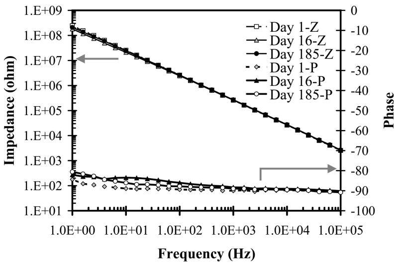
Although the impedance remained greater than 108 Ohms at 1 Hz over the 6 months period test, the impedance and phase underwent a very little change in the low frequency range as shown in Fig. 11. The constant impedance magnitude and nearly −90° phase over time suggests that the film is stable in 37°C Ringer’s solution. The small decrease of the impedance and increase of phase indicates a large resister in parallel with a pure capacitor. These small changes in measured properties might be due to very tiny defects in the film. However, increasing the film density as well as the thickness may further improve the encapsulation property for a critical application. The results further indicate that a-SiCx:H has the potential not only to hermetically encapsulate the biomedical devices, but also to be dielectric passivation layer in a silicon device requiring low process temperature.
Fig. 11.
Impedance spectroscopy plots selected from an over 6-month soaking test. The impedance was denoted by Z and the phase was denoted by P in the figure.
3.6 Dielectric constant
Low dielectric constant material reduces parasitic losses and cross-talk due to resistive- capacitive components coupling and is preferred in dielectric barrier application. Dielectric constant of a-SiCx:H was estimated by impedance spectroscopy to be approximately 4.5, which is close to previous reports [13] and lower than the prevalent dielectric material, silicon nitride of 9. This suggests a-SiCx:H may be an ideal dielectric barrier for neural recording arrays.
3.7 Conformal coating
The SEM micrograph (Fig. 12) revealed the thickness variations of the encapsulation layer along the UEA probe of length 1.2 mm. Film thickness decreases rapidly from average 2.5 μm at the tip to an average of 1.5 μm within approximately 50 μm distance. The encapsulation thickness at middle of the shaft decreased to 0.75 μm. Towards the base of the probe shaft, thickness decreased to about 0.55 μm. Our observations are consistent with the previous report that the deposition rate has been a function of distance from ground electrode [7]. Therefore, we need to take into account the thickness variation to fully insulate the bottom of the shaft and deinsulate the active electrode tip site by reactive ion etching process [29].
Fig. 12.
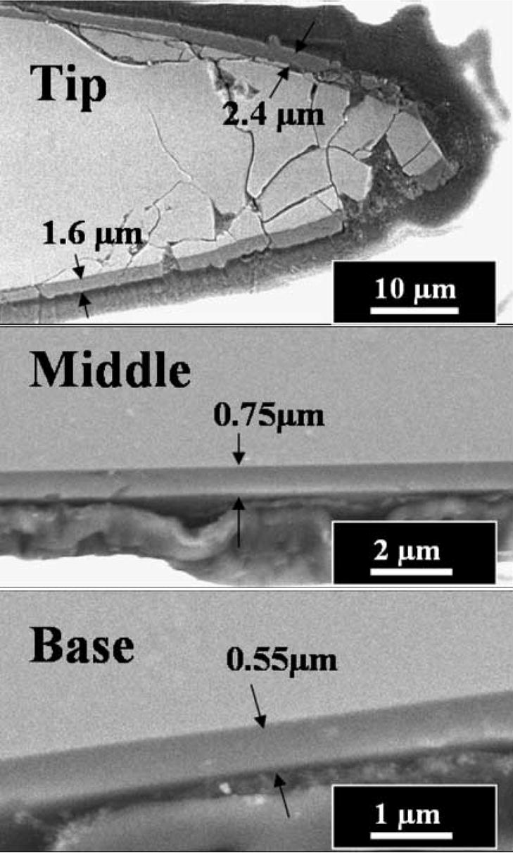
SEM cross-section images of the base, middle and tip part of an electrode from Utah electrode array. a-SiCx:H film thickness measured to be 2.4, 0.75 and 0.55 μm at the tip, middle and base, respectively.
4 Conclusions
We deposited a-SiC:H by PECVD and characterized its encapsulation properties. FT-IR spectra indicated that the Si-C bond density can be controlled even at very low deposition temperatures (Ts<200°C) by altering the hydrogen dilution ratio and precursor ratio. The conditions leading to the highest Si-C bonding density in the ranges of parameters investigated are the temperature of 275°C, the hydrogen dilution of 12.85 and the precursor ratio of 0.17. The encapsulation property may be enhanced with a high Si-C bond density, but the residual film stress must also be considered. When a-SiCx:H was deposited with proper thickness and parameters, it neither dissolved nor generated visible defects after 6 weeks of soaking in 90°C phosphate buffered saline. The impedance remained high during the 6-month impedance spectroscopy test indicating that a-SiCx:H is a promising encapsulation material. In addition, films deposited on silicon substrates at 200°C have low stress allowing further increase of the thickness to improve encapsulation capability. Including the properties of coating conformity and low dielectric constant, this research suggests a-SiCx:H has the potential to hermetically encapsulate biomedical devices at low process temperature. These results suggest that PECVD a-SiCx:H is suitable to be the hermetic encapsulation material for the integrated neural interface devices.
Acknowledgments
This work is supported by NIH contract No. HHSN265200423621C/N01-NS-4-2362 The authors would like to thank Srinivasan Kannan for assistance on the PECVD system, Tzu-Chien Wen and Daniel Ure for the assistance of Impedance spectroscopy measurement. Appreciation is also extended to Dr. Richard Vanfleet, at the Brigham Young University, for assistance on the SEM, and Sascha Kammer, at the Fraunhofer Institute for Biomedical Technology IBMT, for the discussion of some experiments.
Footnotes
FULL POSTAL ADDRESSES
Hsu, Jui-Mei : 50 S. Central Campus Drive, Rm1490, MEB, University of Utah, Salt Lake City, UT84112
Tathireddy, Prashant : 50 S. Central Campus Dr., Rm 3280, Dept. of Electrical Engineering, MEB, University of Utah, Salt Lake City, UT 84112
Rieth, Loren : Rm 227, Kennecott, 1495 East 100 South SLC, UT 84112
Normann, A. Richard : 20 S. 2030 E., Rm. 508F, BPRB, Salt Lake City, UT 84112-9458
Solzbacher, Florian : 50 S. Central Campus Drive, Rm 3116, MEB, University of Utah, Salt Lake City, UT84112
Publisher's Disclaimer: This is a PDF file of an unedited manuscript that has been accepted for publication. As a service to our customers we are providing this early version of the manuscript. The manuscript will undergo copyediting, typesetting, and review of the resulting proof before it is published in its final citable form. Please note that during the production process errors may be discovered which could affect the content, and all legal disclaimers that apply to the journal pertain.
References
- 1.Vaughan TM, Heetderks WJ, Trejo LJ, Rymer WZ, Weinrich M, Moore MM, Kubler A, Dobkin BH, Birbaumer N, Donchin E, Wolpaw EW, Wolpaw JR. IEEE Trans Neural Syst Rehabil Eng. 2003;11:94. doi: 10.1109/tnsre.2003.814799. [DOI] [PubMed] [Google Scholar]
- 2.Donoghue JP. Nat Neurosci. 2002;5(Suppl):1085. doi: 10.1038/nn947. [DOI] [PubMed] [Google Scholar]
- 3.Carmena JM, Lebedev MA, Crist RE, O'Doherty JE, Santucci DM, Dimitrov DF, Patil PG, Henriquez CS, Nicolelis MA. PLoS Biol. 2003;1:E42. doi: 10.1371/journal.pbio.0000042. [DOI] [PMC free article] [PubMed] [Google Scholar]
- 4.Nordhausen CT, Rousche PJ, Normann RA. Brain Res. 1994;637:27. doi: 10.1016/0006-8993(94)91213-0. [DOI] [PubMed] [Google Scholar]
- 5.Jones KE, Campbell PK, Normann RA. Ann Biomed Eng. 1992;20:423. doi: 10.1007/BF02368134. [DOI] [PubMed] [Google Scholar]
- 6.Töpper M, Klein M, Buschick K, Glaw V, Orth K, Ehrmann O, Hutter M, Oppermann H, Becker K-F, Braun T, Kim S, Tathireddy P, Chakravarty S, Solzbacher F. Electronic Components and Technology. Proceedings of the 56th Electronic Components and Technology Conference; San Diego, U.S.A. May 30- June 2, 2006; 2006. p. 705. [Google Scholar]
- 7.Cogan SF, Edell DJ, Guzelian AA, Liu YP, Edell R. J Biomed Mater Res A. 2003;67:856. doi: 10.1002/jbm.a.10152. [DOI] [PubMed] [Google Scholar]
- 8.Fortin JB, Lu T-M. Chemical vapor deposition polymerization: the growth and properties of parylene thin films. Kluwer Academic Publishers; Norwell, MA: 2004. [Google Scholar]
- 9.Loeb GE, Peck RA, Martyniuk J. J Neurosci Methods. 1995;63:175. doi: 10.1016/0165-0270(95)00107-7. [DOI] [PubMed] [Google Scholar]
- 10.Liger M, Rodger DC, Tai Y-C. Micro Electro Mechanical Systems. Proceedings of the IEEE Sixteenth Annual International Conference on Micro Electro Mechanical Systems; Kyoto, Japan. January19–23, 2003; 2003. p. 602. [Google Scholar]
- 11.Zetterling CM. Process Technology for Silicon Carbide Devices. INSPEC The Institution of Electrical Engineers; London, UK: 2002. [Google Scholar]
- 12.Chiang CC, Ko IH, Chen MC, Wu ZC, Lu YC, Jang SM, Liang MS. J Electrochem Soc. 2004;151:G606. [Google Scholar]
- 13.Tsui B, Fang K, Lee S. IEEE Trans Electron Dev. 2001;48:2375. [Google Scholar]
- 14.Summonte C, Rizzoli R, Bianconi M, Desalvo A, Iencinella D, Giorgis F. J Appl Phys. 2004;96:3987. [Google Scholar]
- 15.Desalvo A, Giorgis F, Pirii CF, Tresso E, Rava P, Galloni R, Rizzoli R, Summonte C. J Appl Phys. 1997;81:7973. [Google Scholar]
- 16.Orpella A, Vetter M, Ferre R, Martin I, Puigdollers J, Voz C, Alcubilla R. Sol Energ Mater Sol Cell. 2005;87:667. [Google Scholar]
- 17.Martin I, Vetter M, Orpella A, Puigdollers J, Cuevas A, Alcubilla R. Appl Phys Lett. 2001;79:2199. [Google Scholar]
- 18.Martin I, Vetter M, Orpella A, Voz C, Puigdollers J, Alcubilla R. Appl Phys Lett. 2002;81:4461. [Google Scholar]
- 19.Bolz A, Amon M, Ozbek C, Heublein B, Schaldach M. Tex Heart Inst J. 1996;23:162. [PMC free article] [PubMed] [Google Scholar]
- 20.Amon M, Bolz A, Schaldach M. J Mater Sci Mater Med. 1996;7:273. [Google Scholar]
- 21.Kalnins U, Erglis A, Dinne I, Kumsars I, Jegere S. Med Sci Monit. 2002;8:PI16. [PubMed] [Google Scholar]
- 22.Pereyra I, Villacorta C, Carreno M, Prado R, Fantini M. Braz J Phys. 2000;30:533. [Google Scholar]
- 23.Solomon I, Schmidt MP, Hai TQ. Phys Rev B Condens Matter. 1988;38:9895. doi: 10.1103/physrevb.38.9895. [DOI] [PubMed] [Google Scholar]
- 24.Jean A, Chaker M, Diawara Y, Leung PK, Gat E, Mercier PP, Pepin H, Gujrathi S, Ross GG, Kieffer JC. J Appl Phys. 1992;72:3110. [Google Scholar]
- 25.Demichelis F, Giorgis F, Pirri CF. Solid State Commun. 1995;96:17. [Google Scholar]
- 26.Pereyra I, Carreno M, Tabacniks M, Prado R, Fantini M. J Appl Phys. 1998;84:2371. [Google Scholar]
- 27.Giorgis F, Pirri C, Tresso E, Rava P. Diamond Relat Mater. 1997;6:1606. [Google Scholar]
- 28.Windischmann H. J Vac Sci Technol: Vacuum, Surfaces, and Films. 1991;9:2459. [Google Scholar]
- 29.Padiyath R, Wright RL, Chaudhry MI, Babu SV. Appl Phys Lett. 1991;58:1053. [Google Scholar]


