Fig. 12.

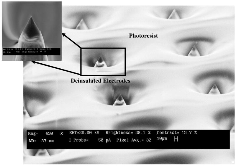
SEM micrograph of electrode array during tip deinsulation. Electrodes tips are exposed in the photoresist, as the photoresist is etched from the tips, Parylene also gets etched. Also shown is magnified image of a single electrode.

SEM micrograph of electrode array during tip deinsulation. Electrodes tips are exposed in the photoresist, as the photoresist is etched from the tips, Parylene also gets etched. Also shown is magnified image of a single electrode.