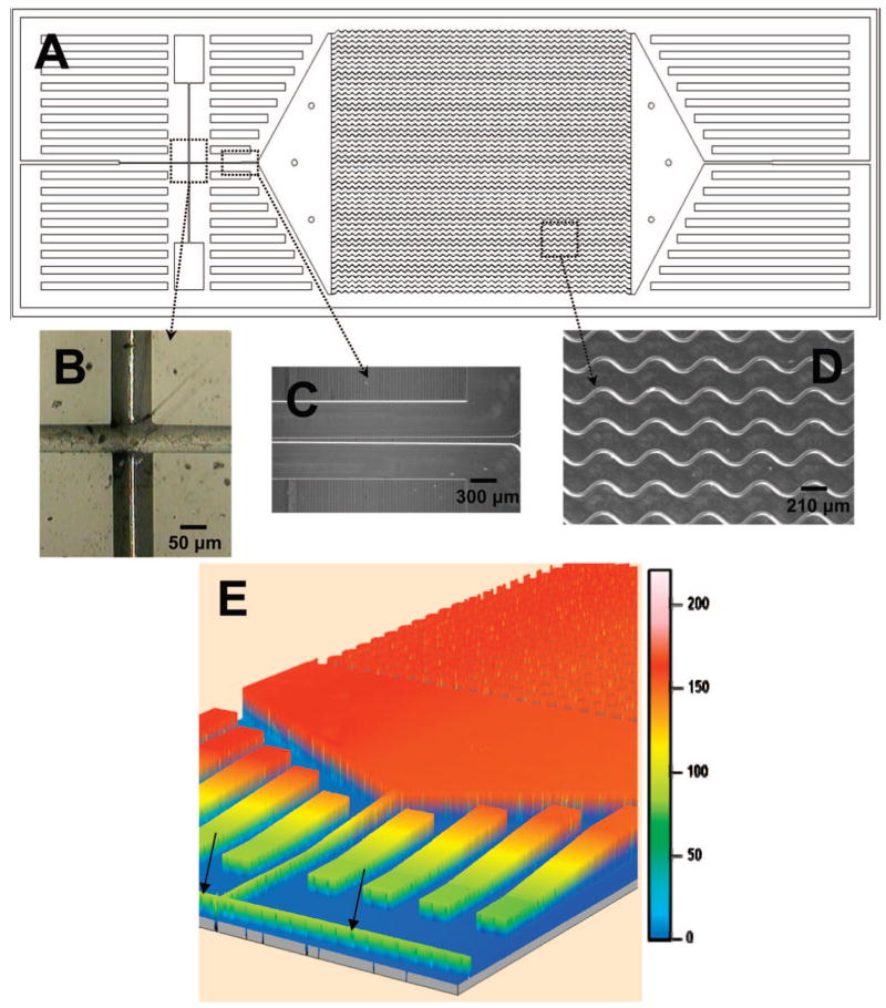
Figure 1.
Schematics of the HTMSU showing the following: (A) A scaled AutoCAD diagram of the sinusoidally shaped capture channels with brightfield optical micrographs of (B) the integrated conductivity sensor consisting of cylindrical Pt electrodes that were 75 μm in diameter with a 50 μm gap and (C) the single port exit where the HTMSU tapers from 100 μm wide to 50 μm while the depth tapers from 150 to 80 μm over a 2.5 mm region that ends 2.5 mm from the Pt electrodes; (D) micrograph taken at 5× magnification showing the sinusoidal cell capture channels; and (E) 3D projection of the topology of the HTMSU obtained at 2.5 μm resolution using noncontact optical profilometry (arrows indicate the Pt electrode conduits).

