Figure 3.

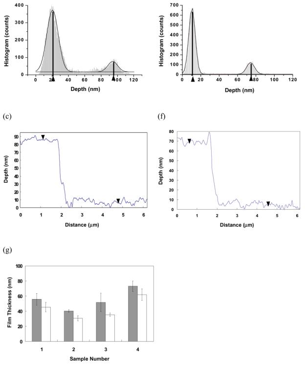
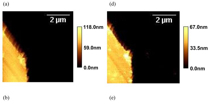
AFM images of a ppNIPAM step on a silicon surface at 25°C (a) and 37°C (d). The corresponding height histograms (gray area) at 25°C (b) and 37°C (e) show two main heights, representing the substrate and plasma polymer surfaces respectively. Each of the peaks is fitted to a Gaussian model (black curve) and the centers of the peaks are denoted by the triangular cursors. The step heights are obtained by subtracting the lower cursor position from the upper, giving a plasma polymer thickness of 73.7 nm at 25°C and 63.7 nm at 37 °C for the scanned region. Section analyses on individual scan lines in each image are shown in (c) for 25°C and (f) for 37°C, which yields step heights of 74.2 nm and 63.1 nm respectively. Film thickness measured on 4 different samples and 3 spots on each samples is summarized in (g) using the histogram analsyis. The gray bar and white bar are film thickness measured at 25°C and 37°C respectively and thicker film is noticed for all measurements at 25°C.

