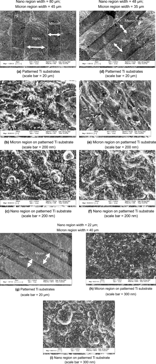
Figure 2.
Scanning electron microscopy images of the (a, d, g) patterned Ti substrates, (b, e, h)micron region of the patterned Ti substrate, and (c, f, i) nano region of the patterned Ti substrate. Nano regions on patterned substrates were created using electron beam deposition and possessed an increased nanometer surface roughness compared with the micron region of the patterned Ti substrates. Bars = (a, d, g) 20 μm; (h, i) 300 nm; (b, c, e, f) 200 nm.

