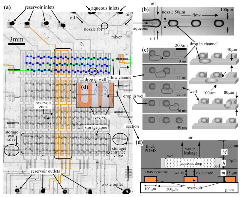
Figure 1.
(a) Plan view of the Phase Chip. (b) Drop formation at nozzle. Confined drops are flattened and elongated in the flow channels. A movie, S4.1, is in the supplement. (c) Photographs of surface tension guided storage of aqueous drops into rectangular wells. Movies are shown in the supplement S4.2, S4.3 and S4.4. These pictures are taken on a chip without a reservoir and have different dimensions than the device portrayed in the rest of this figure. (d) Vertical section of the Phase Chip corresponding to the insert in (a). The device is constructed from two PDMS layers and subsequently sealed together. In the upper, thick (5 mm) layer there are flow channels and storage wells. In the lower, thin (40 μm) layer there is a reservoir sealed by a 15 μm thick PDMS membrane. The reservoir is formed by spin coating a 40 μm thick layer PDMS over a 25 μm high photoresist mold. The principle path for water permeation is between the drop and the reservoir, but there is also a small flux through the 5 mm thick PMDS layer between the drop and the device exterior.

