Abstract
Carbon electrodes are widely used in electrochemistry due to their low cost, wide potential window, and low and stable background noise. Carbon-fiber electrodes (CFE) are commonly used to electrochemically measure “quantal” catecholamine release via exocytosis from individual cells, but it is difficult to integrate CFEs into lab-on-a-chip devices. Here we report the development of nitrogen doped diamond-like carbon (DLC:N) microelectrodes on a chip to monitor quantal release of catecholamines from cells. Advantages of DLC:N microelectrodes are that they are batch producible at low cost, and are harder and more durable than graphite films. The DLC:N microelectrodes were prepared by a magnetron sputtering process with nitrogen doping. The 30 μm by 40 μm DLC:N microelectrodes were patterned onto microscope glass slides by photolithography and lift-off technology. The properties of the DLC:N microelectrodes were characterized by AFM, Raman spectroscopy and cyclic voltammetry. Quantal catecholamine release was recorded amperometrically from bovine adrenal chromaffin cells on the DLC:N microelectrodes. Amperometric spikes due to quantal release of catecholamines were similar in amplitude and area as those recorded using CFEs and the background current and noise levels of microchip DLC:N electrodes were also comparable to CFEs. Therefore, DLC:N microelectrodes are suitable for microchip-based high-throughput measurement of quantal exocytosis with applications in basic research, drug discovery and cell-based biosensors.
Keywords: Diamond-like Carbon, Magnetron sputtering, nitrogen doping, exocytosis, amperometry, bioMEMS, lab-on-a-chip
Introduction
The continuing development of BioMEMS or lab-on-a-chip technologies enables fabrication of microchip devices capable of rapid and high-performance single cell analyses (Chen et al., 2003, Dias et al., 2002, Gao et al., 2004, Li et al., 2004, Park et al., 2005, Sun and Gillis, 2006, Tang and Gao, 2005) (reviewed in(Di Carlo and Lee, 2006)). Microchip electrochemical assays benefit from the increase in signal-to-noise ratio that accompanies electrode miniaturization. Microchip devices also offer potential cost savings from mass production and low consumption of reagents due to their reduced size.
Noble metals such as gold and platinum are commonly used in microfabrication, but carbon electrodes are widely used in electrochemistry due to their low cost and wide potential window for measurements. Carbon is also a biocompatible and chemically inert material. Carbon-fiber electrodes (CFEs) have been extensively used to electrochemically measure secretion of catecholamines from individual chromaffin cells. Chromaffin cells package catecholamines in ∼ 300 nm - diameter intracellular vesicles. Upon stimulation, vesicles fuse with the cell membrane and release their contents in the process of exocytosis. Amperometric recordings from CFEs placed immediately adjacent to these cells exhibit spikes in current that correspond to individual vesicle release events, or quanta.
Recent efforts by our group and others are aimed at making amperometric recordings of quantal exocytosis from cells using microchips in order to increase the throughput and lower the cost of these types of measurements. Unfortunately, carbon fiber electrodes are not compatible with standard microfabrication process. Other efforts of integrating carbon materials with microchip devices such as carbon paste (Martin et al., 2001, Osboum and Lunte, 2001, Rossier et al., 1999), or screen-printed carbon (Wang et al., 2001, Wang and Pumera, 2002) are also not compatible with standard batch processing. In addition, soft carbon films can easily detach from microchips with vigorous cleaning, potentially reducing the ability of devices to be used multiple times. Here we describe the use of diamond-like carbon (DLC) as a robust electrochemical electrode material with excellent electrochemical properties that is easily integrated into standard microfabrication processes.
DLC films are hard, amorphous films with a significant fraction of sp3-hybridized carbon atoms and which can contain a significant amount of hydrogen (Robertson, 1994). DLC can be prepared by ion beam deposition, ion-assisted sputtering from graphite or by laser ablation of graphite. DLC has been used for tribological applications due to its hardness, low coefficient of friction and chemical inertness (Hilden et al., 1990, Sivertsen et al., 1997). A limited number of electroanalytical applications of nitrogen-doped DLC (DLC:N) films have been reported (Zeng et al., 2002). For example, Zeng et al. used scanning voltammetry to demonstrate that sputtered DLC:N films have desirable electrochemical properties such as low background current and wide working window (Zeng et al., 2002). A drawback of undoped DLC films prepared by sputtering is that they are not highly conductive because of the presence of diamond-like sp3 hybridized states. We explored two ways to reduce the series resistance. In one approach we used nitrogen doping in-situ during the deposition process. The increase in the conductivity with nitrogen is believed to be due to the process of sp2-bonded carbon clustering (Gupta et al., 2002) and/or introduction of midgap states within the gap which help to downshift the Fermi level or open the conduction band (Amaratunga et al., 1993, Ronning et al., 1995). Likewise, post-annealing can also further increase the conductivity attributed to the clustering phenomenon mentioned above (Gupta et al., 2002), but this treatment leads to poor adhesion of the film to a glass substrate. A second approach was to deposit DLC:N on top of a highly conductive layer such as chromium or Indium Tin Oxide (ITO), which offers the additional advantage of being transparent. Transparent electrodes are desirable because they allow visualization of cells sitting on top of electrodes using conventional inverted microscopes.
Here we characterize DLC:N electrodes using AFM, Raman spectroscopy and cyclic voltammetry and demonstrate their utility to measure quantal release of catecholamines from chromaffin cells. Our results demonstrate that DLC:N electrodes have excellent electrochemical properties, support attachment of cells to the electrodes, and are an inexpensive alternative to the use of noble metals.
Experimental section
DLC:N deposition and patterning
The DLC:N film was deposited using a magnetron sputtering system (ATC2000, AJA International Inc, North Scituate, MA). A graphite sputter target (Williams Advanced Materials Inc, Buffalo NY) with 99.99% purity, 75 mm in diameter and 3 mm thick was used for DLC:N deposition. Microscope glass slides, 25 mm by 75 mm, 0.9 mm thick, were purchased from Fisher Scientific (Waltham, MA). Silicon wafers were a kind gift from MEMC (St. Charles, MO). All substrates were cleaned by soaking in acetone for about 5 minutes, then sequentially rinsed with methanol, isopropanol and DI water, and then blow dried. Prior to film deposition, the substrates were also sputter cleaned by biasing the substrate holder for ∼1-2 minutes at a pressure of 4 mTorr and a RF power of 40 W. The chamber base pressure was ∼5×10⁻⁷ Torr. Gas flow was regulated by mass-flow controllers. 10 sccm Ar and 10 sccm N2 were fed into the chamber and a deposition pressure of 2 mTorr was maintained for the deposition of DLC:N. The deposition time was 2 hours at a power of 300 W to produce a 200 nm-thick DLC:N film. For the two-layer film approach, an ITO layer was deposited first using an ITO target (In2O3/SnO2, with 10% SnO2 by weight, 75 mm diameter, 3 mm thick, 99.99% purity, Williams Advanced Materials Inc.). Sputtering of the two films was sequential without breaking the vacuum using a multi-target source with independent power supplies. RF sputtering was used for ITO deposition at a radio frequency of 13.56 MHz and a power of 180 W. The 20 sccm argon gas flow was regulated by a mass-flow controller and maintained at a working pressure of 4 mTorr. The deposition temperature was 50 °C and the deposition time was 20 minutes to result in a 100 nm-thick ITO film. The second DLC:N layer was deposited using similar conditions as described above for the single-layer DLC:N film except at a temperature of 100 °C and a film thickness of 100 nm. The thickness of the films was measured using a profiler (Alpha step 200, Tencor, San Jose, CA).
Electrodes were patterned by a lift-off process. Positive photoresist (Shipley S1813) was spin-coated onto the glass slides at 2000 rpm, and then a contact aligner (model 200IR, OAI, San Jose, CA) was used to expose the photoresist using the first transparency mask. After development, the substrate was rinsed with DI water and dried with an air stream. Then the slides were loaded into the sputtering chamber for the ITO/DLC:N double-layer film deposition as described in the previous section. The slides were then soaked in acetone for lift-off. After ∼ 30 minutes, gentle sonication was used to help remove the remaining photoresist.
Device design and fabrication
The layout of the device is depicted in Fig. 1. Eight conducting electrode traces are patterned on a 25 mm by 75 mm glass slide substrate. Each trace consists of a continuous line between two contact pads on opposite sides of the glass slide (Fig. 1A). The traces converge at a 4 mm long center portion of the slide with each trace narrowing from a width of 100 μm to a width of 40 μm near the center of the chip. The traces are covered by a 2 μm thick insulating layer of positive photoresist (Shipley S1813, Microposit, St. Marlborough, MA) except for the contact pads (to allow connection to an external amplifier) and a 30 μm wide opening in the middle to define each of the eight 30 × 40 μm working electrodes. The mask for patterning the photoresist insulation is depicted in Fig. 1B whereas Fig. 1C depicts 4 working electrodes. This design requires only crude alignment between the mask defining the insulating photoresist pattern and the underlying patterned electrodes and therefore can be carried out even without a mask aligner.
Fig. 1.
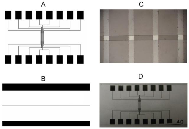
The design of the chip device for cell exocytosis measurement using DLC:N microelectrodes. A. Layout of mask for the lift-off process to pattern the electrodes and contact pads, B. Second mask for patterning insulating photoresist that covers the chip except for the contacts pads at the edge and a 30 μm wide line in the middle to define the working electrodes. C. Photomicrograph displaying 4 DLC:N microelectrodes. Vertical lines are the 40 μm-wide DLC:N conducting traces, whereas the horizontal opening of the photoresist defines the 30 μm by 40 μm working electrodes. D. Photograph of completed chip device on a 25 mm by 75 mm glass slide.
Raman Spectroscopy
We used visible Raman spectrometry (Model HR320, Jobin Yvon Inc., Edison, NJ) with an excitation wavelength of 514.5 nm (EL=2.41 eV) from an Ar+ laser in a backscattered configuration. All of the spectra were measured with a beam spot size ∼ 3 μm with minimum power <5 mW (or intensity ∼ 10 kW/cm2) to avoid thermal degradation to the samples. The first-order Raman spectral data were acquired using a liquid nitrogen cooled back end charged coupled detector (CCD) and were analyzed using Spectramax software (Jobin Yvon, Inc.). All of the Raman spectra were deconvolved wherever needed using Microcal Origin with Peakfit module (ver. 7 or higher, Microcal Inc., Northampton, MA). All of the bands were fitted using the above-mentioned software that employs the Marquardt-Levenberg algorithm to find the absolute minimum of χ2 and maximize the randomness of the residuals.
Exocytosis Measurements
The setup for measuring cell exocytosis is shown schematically in Fig. 2. A small reservoir was created by placing a polydimethylsiloxane (PDMS) gasket with an opening of ∼2 mm by 4 mm on top of the glass chip. An alligator clip was used to make a connection to a contact pad on the chip and a wire connected the clip to the head stage of the EPC-9 patch-clamp amplifier (HEKA, Lambrecht, Germany). Pulse software (HEKA) was used to control the amplifier and acquire data through the built-in A/D interface of the EPC-9. A Ag/AgCl wire was placed into the drop of bath solution (described in the next section) in the reservoir to serve as the reference electrode. For amperometric recording, a +700 mV potential (relative to the Ag/AgCl reference) was applied to the working microelectrode. To minimize pickup of electrical interference, the chip and the head stage were shielded in a Faraday cage.
Fig. 2.
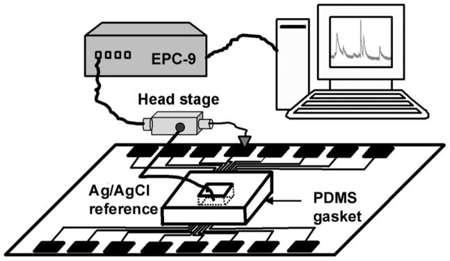
The experimental setup for exocytosis measurement using the EPC-9 patch-clamp amplifier and HEKA pulse software.
Chromaffin cell preparation
Chromaffin cells were harvested from bovine adrenal glands as recently described (Yang et al., 2007). Harvested cells were placed into 25 cm2 polystyrene cell culture flasks at a density of ∼106 cells in 5 mL of culture media (Dulbecco’s modified Eagles medium supplemented with 10% (v/v) fetal bovine serum and 1% penicillin/streptomycin). Cells were kept in a 37 °C incubator in a humidified environment with 5% CO2 and used for a period of 1-4 days after preparation. Immediately before experimentation, cells were removed from the culture flask using a rigorous pipette washing with medium and put into a 10 mL plastic tube. After a gentle centrifugation for about 4 minutes, the supernatant was removed and the cells were gently resuspended in our standard bath solution. Our standard bath solution consisted of (in mM): 150 NaCl, 5 KCl, 5 CaCl2, 2 MgCl2, 10 glucose, and 10 HEPES titrated to pH 7.2 with NaOH. The “high-K+” solution used to stimulate exocytosis consisted of (in mM) 100 KCl, 55 NaCl, 5 CaCl2, 2 MgCl2, 10 HEPES, and 10 glucose. All reagents were obtained from Sigma Aldrich (St. Louis, MO), unless otherwise indicated. The final cell concentration in the standard bath solution was about 106 cells/mL. 10 μL of the cell suspension was loaded into the reservoir on the chip for experimentation. About 10-20 μL of the “high-K+” stimulation solution were added to the reservoir after the cells were allowed to settle for ∼ 5-10 minutes.
Results and Discussion
Properties of sputtered DLC:N film
Surface roughness
Atomic force microscopy (Model Dimension 3100, Veeco Metrology, Inc. Santa Barbara, CA) was used to analyze the surface roughness of the deposited DLC:N films. Figure 3 presents a representative AFM image. The as-deposited DLC:N film on glass has an average grain size of 5 nm and surface roughness of 1.5 nm. DLC:N films deposited on a silicon wafer had an average grain size of 5 nm and surface roughness of 1.4 nm. This excellent surface smoothness explains the mirror-like shiny surface of the deposited DLC:N film and leads to a low specific capacitance of the electrodes.
Fig. 3.
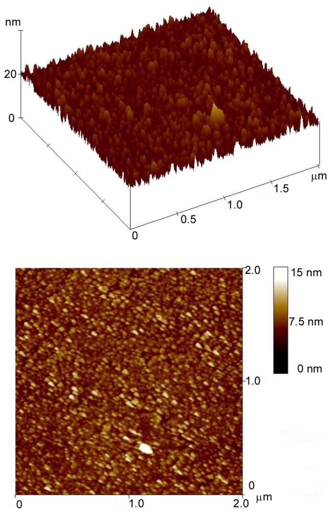
AFM image of the DLC:N film deposited on a glass substrate. The image indicates a very smooth surface and small grain size.
Electrical properties of the DLC:N film
A four-point probe (S302, Lucas Labs, Gilroy, CA) was used to measure the sheet resistance of the as-deposited DLC:N films. A low sheet resistance is desirable in electrochemical electrodes to minimize the series resistance and allow better control of the electrode potential. The results are shown in table 1. The series resistance of each patterned microelectrode is ∼ 4-6 kΩ for the DLC:N/ITO combination. Therefore typical amperometric spkikes with peak amplitude < 1 nA will result in a negligible voltage drop across the series resistance (< 10 μV).
Table 1. Comparison of the electrical properties of single- and dual- layer DLC:N film electrodes.
| Film | Thickness t (nm) | Sheet resistance Rs (Ω/cm2) | Resistivity ρ=Rst (Ω*cm) | Electrode resistance (Ω) |
|---|---|---|---|---|
| DLC:N | 210 | 4.48 × 10⁴ | 0.94 | 3∼4 M Ω |
| DLC:N on ITO | 200 | 126.8 | 2.536 × 10⁻³ | 4∼6 k Ω |
Raman spectroscopy of the DLC:N film
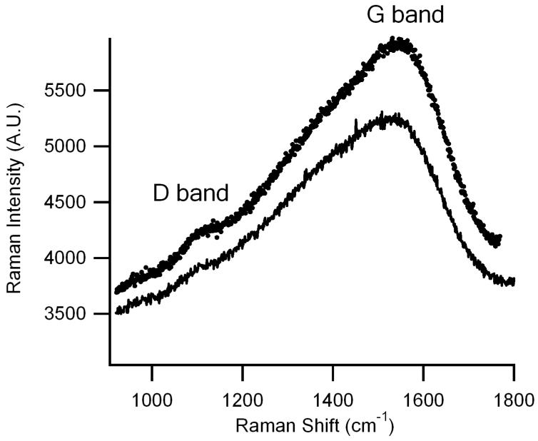
Raman spectroscopy has emerged as one of the most widely used nondestructive analytical tools to probe the structural bonding configurations of carbon-based materials (Dresselhaus and Eklund, 2000, Ferrari and Robertson, 2000, Rao et al., 1997). Spectra obtained from DLC:N films on glass (dark trace) or silicon (light trace) substrates are depicted in Fig. 4. Prominent bands of interest in the first-order Raman spectral regime are D and G bands occurring at ∼ 1340 and 1580 cm-1, respectively (Gupta and Patel, 2007). The high-frequency band (G band) results from graphite (Ulbricht et al., 2002), whereas the D band is due to in-plane substitutional hetero-atoms, vacancies, grain boundaries or other defects (Ferrari and Robertson, 2000). Qualitatively, the broad D and G bands apparent in Fig. 4 indicate that the DC magnetron sputtered DLC:N films appear to be relatively disordered (Zeng et al., 2002).
Fig. 4.
Raman spectroscopic scan of the DLC:N films on silicon and glass substrates. The lighter trace is DLC:N deposited on a silicon substrate whereas the darker trace is for a film deposited on a glass substrate. The broadened G (1580 cm-1) and D (1340 cm-1) peaks indicate that the DLC:N film is highly disordered.
Electrochemical characteristics of the DLC:N microelectrodes
Cyclic voltammetry of the DLC:N film
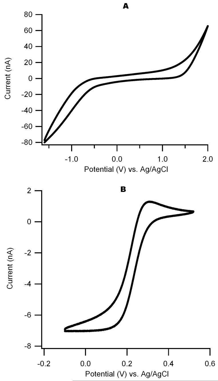
We first checked the working voltage range of the DLC:N electrodes in 100 mM H2SO4 as shown in Fig. 5A. The background current is low and varies little with voltage over a range of ∼-0.8 V to +1.5 V. We next obtained cyclic voltammograms using a standard reversible analyte: 1 mM K3Fe(CN)6 in 0.1 M KCl, pH 3.0. Fig. 5B shows a sample voltammogram (scan rate: 100 mV/s) that exhibits a sigmoidal response with a sharp transition and flat diffusion-limited reduction current, indicative of an appropriately low series resistance. The half-wave reduction potential is 0.24 V versus Ag/AgCl, consistent with previous reports (Schulte and Chow, 1996). The theoretical value of a diffusion limited current (ilim) for a univalent reaction on a disk electrode in an infinite plane is given by (Bard and Faulkner, 2001):
where D is the diffusion coefficient, C is the concentration, F is Faraday’s constant and r is the radius of the electrode. If we assume the “effective radius” of our 40 × 30 μm rectangular electrode is equal to half the diagonal length, i.e., 25 μm, and a diffusion coefficient of 7.2×10⁻⁶ cm2/s, then the theoretical value of ilim is 6.95 nA. Note that the measured value of ilim from Fig. 5B is ∼ 7 nA, suggesting the working electrode has the expected active area.
Fig. 5.
Cyclic voltammograms of the DLC:N film electrode. The working electrode size is 30 μm by 60 μm. A. cyclic voltammogram in 100 mM H2SO4, scan rate 0.1V/s, shows a large working window. B. Cyclic voltammogram of 1 mM K3Fe(CN)6 in 0.1 M KCl, pH 3.0, scan rate 0.1 V/s.
Background current, specific capacitance and noise of DLC:N microelectrodes
The background current measured from our DLC:N microelectrodes during amperometric measurements in our standard cell bath solution varied over a range from 20 - 200 pA in freshly fabricated, properly insulated devices measured several minutes after stepping the potential to 0.7 V versus Ag/AgCl (e.g., see Fig. 6). One reason for the variability in our measurement of background current is because this current continues to decay for tens of minutes after changing the electrode potential. This background current (∼ 0.02 - 0.16 pA/μm2) is within the range that is typically encountered with carbon fiber microelectrodes (e.g., (Chow and Rüden, 1995)), and lower than what we found for Pt electrodes fabricated and insulated in a similar manner as our DLC:N electrodes (∼0.5 pA/μm2). The capacitance of electrodes ranged from 126 - 146 pF, therefore the specific capacitance (capacitance per unit area) for our DLC:N electrodes is ∼ 11 μF/cm2. This is lower than what has been reported for a beveled carbon-fiber electrode encased in a glass pipette (Kawagoe et al., 1991), but larger than what was reported previously for a DLC:N film (Zeng et al., 2002), perhaps because of differences in the buffers used.
Fig. 6.
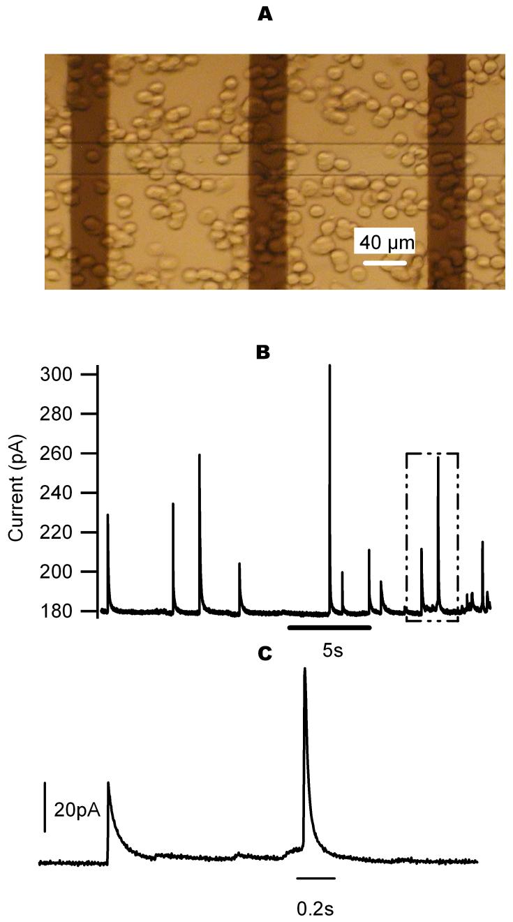
Quantal exocytosis from chromaffin cells recorded on DLC:N microelectrodes. A. Photomicrograph of cells sitting on top of microchip. The vertical dark stripes (40 μm wide) are the DLC:N film electrodes whereas the horizontal line is the opening of the photoresist insulation. The intersection of the vertical and horizontal stripes defines the area of the 3 working electrodes in the photograph. Note that the DLC:N on ITO film is transparent enough to visualize cells through the electrodes using an inverted microscope. B. Amperometric spikes indicative of quantal release of catecholamines from cells on top of electrodes. C. An enlarged view of the portion of B indicated by the dashed box. Each spike indicates oxidation of the contents of an individual granule. Exocytosis was triggered by application of a high K+ solution.
We next measured the current noise of our DLC:N microelectrodes under the same conditions described above with careful attention paid to shield pickup of 60 Hz interference. The standard deviation of current noise is typically 1.1 - 1.6 pA for a bandwidth of 1 kHz, whereas the noise originating from the amplifier is only ∼0.2 pA. Since the standard deviation of the current for amperometric recordings typically scales with the working electrode area (e.g., (Chen et al., 2003)), this corresponds to a noise level of ∼ 1 fA/μm2, which compares favorably with the noise of carbon-fiber microelectrodes (generally less than instrument noise, therefore < 10 fA/μm2) or with Au electrodes (∼ 40 fA/μm2 for a bandwidth of 3 kHz, (Chen et al., 2003)) or Pt electrodes fabricated by our group (∼ 8 fA/μm2).
Amperometric detection of quantal exocytosis of catecholamines from chromaffin cells
Bovine adrenal chromaffin cells were seeded onto the microelectrodes by pipetting a ∼10 μL drop of solution containing ∼106 cells/mL onto the chip. The cells were allowed to settle down to the electrode surface for about 5-10 minutes before recording. Fig. 6A is a photomicrograph of cells settled on the chip imaged through an inverted microscope (Olympus, model IX51). We found that cells adhered better to the DLC:N electrode surface than to similarly prepared Pt or Indium-Tin-Oxide microelectrodes. After cells settled down to the electrodes, recordings were made from electrodes where 1 or 2 cells were sitting directly over the working electrode such as the case of the left-most electrode in Fig. 6A. Typically only ∼20% of the electrodes satisfied this recording condition. Catecholamine release was stimulated by adding 10 μL of the high-K+ solution defined in the Experimental Section. Elevation of the extracellular K+ concentration causes cell depolarization, opening of voltage-gated Ca2+ channels, Ca2+ influx and Ca2+-triggered exocytosis. Fusion of a catecholamine-containing granule immediately adjacent to a working electrode results in a spike of faradaic current as catecholamines are oxidized on the electrode surface (Fig. 6B). In contrast, no amperometric spikes were observed from cells over a several-minute interval before adding the high-K+ solution (data not shown). Amperometric current was low-pass filtered at a cut-off frequency of 1 kHz and sampled at a frequency of 4 kHz. We analyzed 66 amperometric spikes from a continuous recording of 144 seconds using spike analysis software by Segura et al. (Segura et al., 2000). The average rise time is 2.9±0.3 ms with a median value of 2.4 ms, and the average charge per spike is 1.2±0.1 pC. The mean width at half-maximal amplitude of the spikes is 12.3±1.3 ms with a median value of 8.2 ms, whereas the mean spike amplitude is 34.1±3.3 pA. These values are comparable to those found in chromaffin cells using carbon fiber microelectrodes (Chow et al., 1992, Jankowski et al., 1992, Wightman et al., 1991).
Conclusions
DLC:N electrodes have been developed and integrated onto glass slide microchips through a DC magnetron sputtering and lift-off process. The DLC:N microelectrodes exhibit desirable electrochemical properties such as low noise, a small and stable background current, and low capacitance. DLC:N also supports cell adhesion, is biocompatible, inexpensive, and can be deposited using commonly available microfabrication equipment. Amperometric measurements of quantal catecholamine release from chromaffin cells on DLC:N electrodes showed characteristics similar to previous measurements carried out using carbon fiber electrodes. DLC:N thus represents an attractive electrode material to be integrated into future devices that allow automated positioning of cells over microelectrodes for high throughput electrochemical measurement of quantal exocytosis.
Acknowledgement
This work was supported by NIH NS048826.
References
- Amaratunga GAJ, Veerasamy VS, Davis CA, Milne WI, Mckenzie DR, Yuan J, Weiler M. Journal of Non-Crystalline Solids. 1993;166:1119. [Google Scholar]
- Bard AJ, Faulkner LR. Electrochemical Methods: Fundamentals and Applications. Wiley & Sons; New York: 2001. [Google Scholar]
- Chen P, Xu B, Tokranova N, Feng X, Castracane J, Gillis KD. Anal Chem. 2003;75:518. doi: 10.1021/ac025802m. [DOI] [PubMed] [Google Scholar]
- Chow RH, Rüden L.v. In: Single Channel Recording. Sakmann B, Neher E, editors. Plenum Press; New York: 1995. p. 245. [Google Scholar]
- Chow RH, von Ruden L, Neher E. Nature. 1992;356:60. doi: 10.1038/356060a0. [DOI] [PubMed] [Google Scholar]
- Di Carlo D, Lee LP. Anal Chem. 2006;78:7918. doi: 10.1021/ac069490p. [DOI] [PubMed] [Google Scholar]
- Dias AF, Dernick G, Valero V, Yong MG, James CD, Craighead HG, Lindau M. Nanotechnology. 2002;13:285. [Google Scholar]
- Dresselhaus MS, Eklund PC. Advances In Physics. 2000;49:705. [Google Scholar]
- Ferrari AC, Robertson J. Physical Review B. 2000;61:14095. [Google Scholar]
- Gao J, Yin XF, Fang ZL. Lab Chip. 2004;4:47. doi: 10.1039/b310552k. [DOI] [PubMed] [Google Scholar]
- Gupta S, Patel RJ. Journal of Raman Spectroscopy. 2007;38:188. [Google Scholar]
- Gupta S, Weiner BR, Morell G. Applied Physics Letters. 2002;80:1471. [Google Scholar]
- Hilden M, Lee J, Nayak V, Ouano G, Wu A. IEEE Transactions on Magnetics. 1990;26:174. [Google Scholar]
- Jankowski JA, Schroeder TJ, Holz RW, Wightman RM. J Biol Chem. 1992;267:18329. doi: 10.21236/ada251716. [DOI] [PubMed] [Google Scholar]
- Kawagoe KT, Jankowski JA, Wightman RM. Anal Chem. 1991;63:1589. doi: 10.1021/ac00015a017. [DOI] [PubMed] [Google Scholar]
- Li PC, de Camprieu L, Cai J, Sangar M. Lab Chip. 2004;4:174. doi: 10.1039/b400770k. [DOI] [PubMed] [Google Scholar]
- Martin RS, Gawron AJ, Fogarty BA, Regan FB, Dempsey E, Lunte SM. Analyst. 2001;126:277. doi: 10.1039/b009827m. [DOI] [PubMed] [Google Scholar]
- Osboum DM, Lunte CE. Anal Chem. 2001;73:5961. doi: 10.1021/ac010496i. [DOI] [PMC free article] [PubMed] [Google Scholar]
- Park J, Jung SH, Kim YH, Kim B, Lee SK, Park JO. Lab Chip. 2005;5:91. doi: 10.1039/b404990j. [DOI] [PubMed] [Google Scholar]
- Rao AM, Richter E, Bandow S, Chase B, Eklund PC, Williams KA, Fang S, Subbaswamy KR, Menon M, Thess A, Smalley RE, Dresselhaus G, Dresselhaus MS. Science. 1997;275:187. doi: 10.1126/science.275.5297.187. [DOI] [PubMed] [Google Scholar]
- Robertson J. Pure and Applied Chemistry. 1994;66:1789. [Google Scholar]
- Ronning C, Griesmeier U, Gross M, Hofsass HC, Downing RG, Lamaze GP. Diamond and Related Materials. 1995;4:666. [Google Scholar]
- Rossier JS, Schwarz A, Reymond F, Ferrigno R, Bianchi F, Girault HH. Electrophoresis. 1999;20:727. doi: 10.1002/(SICI)1522-2683(19990101)20:4/5<727::AID-ELPS727>3.0.CO;2-A. [DOI] [PubMed] [Google Scholar]
- Schulte A, Chow RH. Analytical Chemistry. 1996;68:3054. doi: 10.1021/ac960210n. [DOI] [PubMed] [Google Scholar]
- Segura F, Brioso MA, Gomez JF, Machado JD, Borges R. Journal of Neuroscience Methods. 2000;103:151. doi: 10.1016/s0165-0270(00)00309-5. [DOI] [PubMed] [Google Scholar]
- Sivertsen JM, Wang G, Chen GL, Judy JH. IEEE Transactions On Magnetics. 1997;33:926. [Google Scholar]
- Sun XH, Gillis KD. Analytical Chemistry. 2006;78:2521. doi: 10.1021/ac052037d. [DOI] [PubMed] [Google Scholar]
- Tang H, Gao YF. IEEE Sensors Journal. 2005;5:1346. [Google Scholar]
- Ulbricht H, Moos G, Hertel T. Physical Review B. 2002;66:075404. doi: 10.1103/PhysRevLett.90.095501. [DOI] [PubMed] [Google Scholar]
- Wang J, Chatrathi MP, Tian B. Anal Chem. 2001;73:1296. doi: 10.1021/ac001205t. [DOI] [PubMed] [Google Scholar]
- Wang J, Pumera M. Anal Chem. 2002;74:5919. doi: 10.1021/ac020416q. [DOI] [PubMed] [Google Scholar]
- Wightman RM, Jankowski JA, Kennedy RT, Kawagoe KT, Schroeder TJ, Leszczyszyn DJ, Near JA, Diliberto EJ, Jr., Viveros OH. Proc Natl Acad Sci U S A. 1991;88:10754. doi: 10.1073/pnas.88.23.10754. [DOI] [PMC free article] [PubMed] [Google Scholar]
- Yang Y, Craig TJ, Chen X, Ciufo LF, Takahashi M, Morgan A, Gillis KD. J Gen Physiol. 2007;129:233. doi: 10.1085/jgp.200609685. [DOI] [PMC free article] [PubMed] [Google Scholar]
- Zeng A, Liu E, Tan SN, Zhang S, Gao J. Electroanalysis. 2002;14:1110. [Google Scholar]


