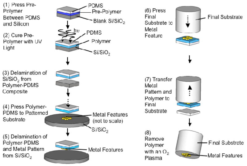
Figure 1.
Schematic of the procedure for transferring metallic nano-structures: (1) press the thiol-ene monomer solution between a featureless silicon wafer and extracted PDMS, (2) UV cure the thiol-ene monomer solution to make a thin thiol-ene film, (3) delaminate the film-PDMS composite from the silicon in a DI water bath, (4) press the thiol-ene film-PDMS composite against a metallic nano-pattern (not shown to scale), (5) delaminate the film-PDMS composite and the attached metal features from the silicon substrate in a DI water bath, (6) press the desired substrate (shown here as a cylinder) against the metallic pattern, (7) transfer the pattern and thiol-ene film to the final substrate, (8) remove the thiol-ene film with an O2 plasma

