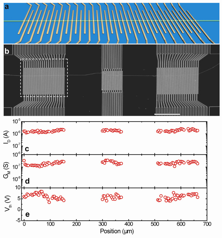
Figure 3.
(a) Schematic of multiple FET array on a single ultra-long p-SiNW. (b) Dark-field optical image of multiple FETs defined by electron beam lithography. The p-SiNW is horizontal in the image and the vertical lines crossing the NW correspond to S/D electrodes with 2 µm width/2 µm separation; scale bar is 100 µm. The dashed white rectangle corresponds to a similar area shown schematically in (a). (c) Position vs. ID at VD= 1V and VG = −10 V measured from the multiple FETs defined on the single p-SiNW in the image. (d) Position vs. GM at VD = 1V. (e) Position vs. Vth.

