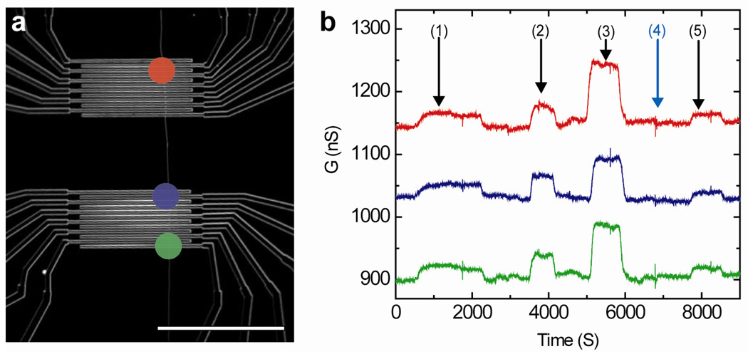
Figure 4.
(a) Optical image of a multiple sensor array with similar source-drain dimensions as in Figure 3b; scale bar, 100 µm. The red, blue and green circles highlight regions from which sensing data were recorded. (b) Conductance-versus-time data measured simultaneously from three FET devices from the red, blue and red regions of the device array. The SiNW FET array was functionalized with mAb for PSA, and the data were recorded by alternating delivery of target solutions (PSA or BSA) and buffer solution where vertical arrows correspond to the delivery of (1) 20 pg/ml PSA, (2) 500 pg/ml PSA, (3) 10 ng/ml PSA, (4) 10 µg/ml BSA, and (5) 20 pg/ml PSA solutions. The functionalization and measurement procedures were the same as reported previously.13,17

