Fig. 2.
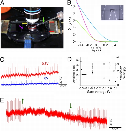
Measurement of cardiomyocyte signals. (A) Photograph of the experimental setup showing the PDMS piece (red dashed box) on top of a NWFET chip within a solution well that is temperature-regulated with an integrated heater (blue arrow). Additional yellow, purple, green, and red arrows highlight positions of the Ag/AgCl reference electrode, solution medium well (length × width × depth = 25–30 × 15–20 × 2 mm3), glass manipulator/force pipette connected to x-y-z manipulator, and plug-in connectors between NWFET interconnect wires and measurement electronics, respectively. (Scale bar, 10 mm.) (B) Representative gate responses of 3 Si NWFET devices. The sensitivity (G/Vg) of the separate devices represented by the green, cyan, and purple traces at Vg = −0.3 V are 13.8, 17.2, and 31.1 nS/mV, respectively. (Inset) Optical microscopy image of a 2 NWFET devices (dashed box) as illustrated schematically in Fig. 1. (Scale bar, 20 μm.) (C) Conductance vs. time traces recorded at Vg = −0.3 V (red) and 0 V (blue) for the same NWFET–cardiomyocyte interface; the device sensitivities at −0.3 and 0 V were 9.2 and 3.5 nS/mV, respectively. (D) Plots of peak conductance amplitude (filled triangles) and calibrated peak voltage amplitude (open squares) vs. Vg; data were obtained from the same experiments shown in C. Error bars correspond to ±1 SD. (E) Conductance vs. time data recorded as PDMS cardiomyocyte substrate was retracted from the NWFET chip (up arrow) and then brought back into contact with the device chip (down arrow).

