Abstract
The response of a compact photonic immunoassay biosensor based on a planar waveguide to variation in antigen (C-reactive protein) concentration as well as waveguide ridge height has been investigated. Near-field scanning optical microscope measurements indicate 1.7%∕nm and 3.3%∕nm top surface optical intensity modulation due to changes in effective adlayer thickness on waveguides with 16.5 and 10 nm ridge heights, respectively. Beam propagation method simulations are in good agreement with the experimental sensitivities as well as the observation of leaky mode interference both within and after the adlayer region.
Label-free immunosensors that can directly sense changes in optical absorption or refractive index due to antigen binding to immobilized antibodies without additional reagents offer benefits of simplified testing, lower operating costs, and reduced interference with target function. Label-free immunoassay biosensors based on optical waveguides include grating couplers,1 Mach–Zehnder interferometers,2 microcavity,3 and surface plasmon sensors.4 However, each of these methods relies on measuring the phase or amplitude of light at the end of the waveguide after it has left the immobilized antibody region where the adlayer forms due to target binding. Such geometries restrict sensors to unambiguously detecting a single analyte per waveguide. In contrast, the local evanescent array coupled (LEAC) biosensor has been specifically designed to measure adlayer thickness using evanescently coupled photodetectors in proximity to the antibody region, allowing simultaneous detection of multiple analytes along a single waveguide. Additionally, the LEAC biosensor has lower sensitivity to temperature than high-Q resonant cavity approaches, and it does not require complex system components such as tunable laser sources or high resolution spectrum analyzers, and can be operated with a light emitting diode source if desired.
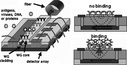
The structure and operating principles of the LEAC biosensor are illustrated in Fig. 1. The increased refractive index due to adlayer formation above the core shifts the field profile of the guided mode in the asymmetric waveguide upward, reducing coupling to the photodetector directly underneath the adlayer. The field shift phenomenon in a proof-of-concept configuration without the underlying detector array is analyzed using a near-field scanning optical microscope (NSOM). Similar to the buried detector array, NSOM directly measures the evanescent field strength and thus the optical intensity, but on the upper surface of the waveguide. Prior successful experiments have been reported on various inorganic5 and photoresist pseudoadlayers.6 In this paper, the optical field responses of the sensor to actual immunoassay complexes with varying antigen coverage, and thus effective adlayer thickness, is reported. Also, the effect of waveguide ridge height on response strength is investigated, and leaky mode interference oscillations in the adlayer region are observed. Beam propagation method (BPM) simulations are in agreement with measured variations due to changes in adlayer thickness and ridge height and also capture the leaky mode interference.
Figure 1.
Schematic of the LEAC sensor.
The SiNx–SiO2 waveguides were fabricated using traditional sputtering, optical lithography, and etching methods. A 105-nm-thick SiNx film was deposited on a SiO2–Si wafer using NH3∕argon sputtering. The SiO2 cladding thickness is approximately 2 μm. Air serves as the upper cladding of the asymmetric structure. The ridge waveguide core is laterally defined by partially dry etching the surrounding SiNx layer in a CF4∕O2 plasma to a depth of 16.5 nm for the thick ridge sample or 10 nm for the thin ridge sample. The waveguide ridges are approximately 2 μm wide. Sample edges were polished for end-fire coupling of a λ0=654 nm wavelength laser diode via visible single-mode fiber (4∕125 μm core∕cladding diameter).
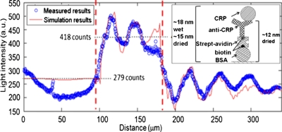
Adlayers composed of a multiple component immunoassay complex were patterned on the waveguide surface. The adlayer consists of biotinylated bovine serum albumin, streptavidin, anti-CRP (C-reactive protein) and CRP layers, as illustrated in the inset of Fig. 2. Each component of the immunoassay complex was attached to the surface by sequentially flowing an associated solution through microchannels in a polydimethylsiloxane (PDMS) mask temporarily attached to the sample surface. For the first experiment, a single 80-μm-wide channel was used to create a 15-nm-thick adlayer on the thin, 10-nm-tall ridge sample. In a second experiment, 11.6-, 12.4-, and 14.8-nm-thick adlayers were formed in three different 40-μm-wide channels on the thick, 16.5-nm-tall ridge sample by varying the concentration of CRP in solution. Table 1 lists the different CRP and ridge height combinations, and the resulting adlayer thicknesses and field modulations. After adlayer formation, the PDMS pieces were removed and films dried in air prior to NSOM measurements. The PDMS blocked the formation of adlayers outside the channels.
Figure 2.
Light intensity along the waveguide. The adlayer (shown in the inset) is present in the region between the two dashed lines.
Table 1.
CRP concentration∕adlayer thickness vs intensity.
| CRPconcentration | Ridgeheight | Adlayerthickness | Intensitymodulation |
|---|---|---|---|
| 1 mg∕ml | 10 nm | 15 nm | 49% |
| 0 μg∕ml | 16.5 nm | 11.6 nm | 18.23% |
| 0.6 μg∕ml | 16.5 nm | 12.4 nm | 19.92% |
| 0.6 mg∕ml | 16.5 nm | 14.8 nm | 23.27% |
The thin ridge sample and thick ridge sample with varying adlayer thicknesses were measured with NSOM to determine the effects of varying ridge height and adlayer thickness. For the thin ridge sample with a single adlayer, a sequence of overlapping 20×100 μm2 optical intensity scans along the waveguide were obtained covering approximately 90 μm before the 80 μm wide adlayer and 170 μm after it. The scan repeatability of optical fields was good in the overlap areas. The measured optical intensity in the waveguide is shown in Fig. 2.
The 15-nm-thick adlayer causes the detected evanescent field power to shift from P0=279 counts immediately before the adlayer to an average Padlayer=418 counts during the adlayer, corresponding to an intensity modulation of (Padlayer−P0)∕P0=+49%. Note that although the NSOM tip has moved away from the SiNx waveguide core above the adlayer, the measured optical power in the evanescent field at the surface of the adlayer is larger, demonstrating the field redistribution locally in the adlayer region that is the operating principle of the LEAC sensor.5 Negative intensity modulation has been observed in relatively thick, 130 nm photoresist artificial adlayers.6 In addition to the shift in average field, oscillation resulting from beating of the different propagation constants of the guided mode and leaky modes is observed after the adlayer region with a beat wavenumber of 0.157∕ μm and in the adlayer region with a beat wavenumber of 0.233∕ μm.
A two-dimensional BPM simulation of the surface field intensity, superimposed on the measured data in Fig. 2, agrees well with the experimental results. The incident beam was assumed to be the fundamental TE mode due to the higher scattering loss of the TM mode. The calculated values for the effective index of the guided and first leaky mode in the adlayer were and corresponding to a beat period of , while the guided and leaky mode effective indices outside of the adlayer were and corresponding to a beat period of . The normal and adlayer regions’ calculated beat periods are in reasonable agreement with the observed values of 27 and 40 μm. Note that the leaky mode effective index is less than that of SiO2 (n=1.45), allowing the leaky mode to radiate into the lower cladding.
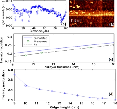
Measurements on the second, thick (16.5 nm) ridge sample with three adlayer regions formed with different CRP concentrations were used to investigate the optical field response to different adlayer thicknesses. As an example, Fig. 3a shows the topographical results of the adlayer with an average thicknesses of 11.6 nm formed in the absence of CRP. The bright spots in the image correspond to high points presumed to be processing defects, residue, dust, or other surface contamination. The high points lift the NSOM tip away from the main surface but are too small to significantly affect the local evanescent field distribution and thus decrease the optical intensity at these points. As a result, the optical intensity averaged across the waveguide width, as shown in Fig. 3b, has sharp dips correlated with the bright spots that occur on the waveguide. To improve data analysis of the intensity profiles, intensity data is excluded at positions corresponding to topological points more than 4 nm above the waveguide ridge and adlayer, which are shown with open circles in Fig. 3b. The remaining filtered data are shown with the solid circles. Least squared linear fits, shown with the dotted lines, are made to the filtered data in the region before and within each adlayer region to determine the optical modulation, i.e., increase in measured average intensity associated with each adlayer thickness. The local evanescent field modulation increases with increasing adlayer thickness as tabulated in Table 1. The total adlayer thickness varies by ∼3 nm, corresponding to the dimensions of CRP, and results in a 5% difference in intensity modulation.
Figure 3.
(a) Topography of a 11.6-nm-thick immunoassay complex without CRP. (b) Light intensities along the waveguide for clean areas (filled circles) and topographic high points that are not included in the fit (open circles). (c) Measured light intensity modulation and BPM simulation results with different adlayer thickness on 16.5-nm-tall ridge. (d) Light intensity modulation vs ridge height for approximately 15-nm-thick adlayers according to 2D BPM simulations (stars and dashed line) and measured data (open circles).
Two-dimensional BPM simulation results of the light intensity modulation above the waveguide with different adlayer thicknesses are shown in Fig. 3c. The incident beam was assumed to be the fundamental TE mode. The simulations indicate a 5% change in intensity modulation for the 3 nm thickness variation, consistent with the measured results, although the absolute simulated modulation with respect to zero adlayer height is 2% higher than the absolute modulation measurements. The slight difference may be caused by the rough topology increasing the effective height of the NSOM tip above the waveguide surface.
For the waveguide with thicker ridge height, the light modulation is much lower than the one with thinner ridge height. These results indicate that decreased waveguide ridge heights enhance sensitivity to adlayer thickness changes. BPM simulations of intensity modulation response to 15-nm-thick adlayers, shown in Fig. 3d, indicate the same trend and are in excellent agreement with the measured results. The expected top surface intensity modulation is predicted to be 10% for 3 nm thickness changes on a waveguide with a 10 nm ridge height.
The response of a LEAC biosensor to immunoassay adlayers has been measured with NSOM to probe the top surface evanescent field response on an asymmetric planar waveguide. For a 16.5-nm-high ridge, varying concentrations of CRP resulted in a 3 nm variation in height and a 5% variation in optical intensity on the top surface corresponding to a modulation sensitivity of 1.7%∕nm. The response to a 15-nm-thick immunoassay adlayer on a 10-nm-high ridge waveguide was approximately twice that of a comparable thickness adlayer on the 16.5 nm ridge height waveguide, corresponding to an increased sensitivity of 3.3%∕nm for the shorter ridge. The mechanism for increasing response to adlayers with smaller ridge height is still under investigation but likely relates to three-dimensional effects associated with the relative strengths of vertical and horizontal index confinement. BPM simulations were in good agreement with the measured sensitivities and also duplicated the interference signals between the guided and leaky modes in both the adlayer region as well as after it. Computer simulation indicated that buried detectors will exhibit larger intensity modulation than the top surface evanescent field.
Acknowledgments
The authors thank A. Van Orden for access to NSOM equipment and Robert Pownall for advice. This work was supported by National Institutes of Health Grant No. EB00726.
References
- Brandenburg A. and Gombert A., Sens. Actuators B 17, 35 (1993). [Google Scholar]
- Heideman R. G., Kooyman R. P. H., Greve J., and Altenburg B. S. F., Appl. Opt. 30, 12 (1991). [DOI] [PubMed] [Google Scholar]
- Krioukov E., Klunder D. J. W., Driessen A., Greve J., and Otto C., Opt. Express 27, 512 (2002). [DOI] [PubMed] [Google Scholar]
- Harris R. D. and Wilkinson J. S., Sens. Actuators B 10.1016/0925-4005(95)01692-9 29, 261 (1995). [DOI] [Google Scholar]
- Yuan G., Stephens M. D., Dandy D. S., and Lear K. L., IEEE Photonics Technol. Lett. 10.1109/LPT.2005.858151 17, 2382 (2005). [DOI] [Google Scholar]
- Yuan G., Stephens M. D., Dandy D. S., Gerding J., Van Orden A., and Lear K. L., Conference on Lasers and Electro-Optics, 2006. (unpublished).


