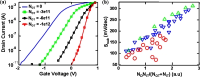
Figure 5.
Device simulations indicating the effect of surface adsorbed charges for the device schematic shown in Fig. 1. (a) Effect of varying adsorbed surface charge density (NOT) with interfacial trap density (NIT) set to 1×10¹² eV−1 cm−2. As the magnitude of surface adsorbed charges is increased, the Ssub improves along with the change Vth. (b) Linear correlation between Ssub and NDNIT∕(NOT+NIT) with different channel doping densities (ND) values of ND=4×1017 cm−3 (triangles), ND=3×1017 cm−3 (inverted triangles), and ND=2×1017 cm−3 (circles).

