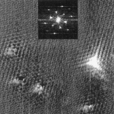
Figure 1.
An image of graphite fluorinated at 300°C obtained with a C60-functionalized STM tip. The prominent 3-fold defect in the lower right is attributed to a covalent C–F bond, whereas the other defects represent fluorine atoms adsorbed with an ionic bond. The spacing between the atomic sites in the unperturbed areas of the image is 2.46 Å. (Inset) Fourier transform of the topographic image. The six outer peaks are caused by the graphite lattice, whereas the six inner peaks correspond to the electronic superlattice. The tunneling parameters were 1-nA and +100-mV sample bias voltage.

