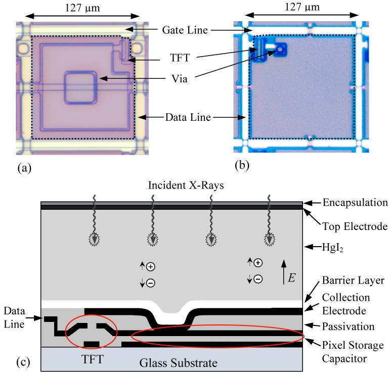
Figure 1.
Microphotographs of the top surface of: (a) an ND10 pixel, and (b) an MD88 pixel. These images were acquired prior to the deposition of the materials comprising a HgI2 detector (i.e., the barrier layer, the photoconductor, the top electrode, and an encapsulation layer). The dashed lines superimposed on the photos indicate the periphery of the signal collection electrode, (c) Schematic cross-sectional view of an ND10 pixel with a HgI2 detector - where the drawing has not been made to scale in order to better illustrate various features of the pixel designs. The cross-sectional view for an MD88 pixel would generally look the same except that the collection electrode also serves as the top electrode of the pixel storage capacitor and this electrode is connected by a via to the drain contact of the TFT. Note that, in this drawing, the depression illustrated in the otherwise planar collection electrode corresponds to an ~40×40 μm2 large, ~2.6 μm deep depression located on the surface of the bare ND10 pixel - a feature that is located at the position of the via indicated in (a).

