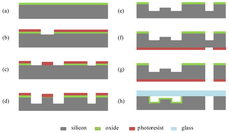
Fig. 2.
Simplified process flow for the microfluidic reactor array device (a) growing a thermal oxide layer; (b) defining the microreactor pattern to PR and thermal oxide layers; (c) defining the microchannel pattern to PR and thermal oxide layers; (d) etching a silicon wafer to create microchannels; (e) etching a silicon wafer to create microreactors; (f) defining the through inlet/outlet hole pattern to the backside of the wafer; (g) etching a silicon wafer to create the through-holes and (h) growing a thermal oxide and bonding to a glass wafer.

